Continue to Site

Welcome to EDAboard.com

Welcome to our site! EDAboard.com is an international Electronics Discussion Forum focused on EDA software, circuits, schematics, books, theory, papers, asic, pld, 8051, DSP, Network, RF, Analog Design, PCB, Service Manuals... and a whole lot more! To participate you need to register. Registration is free. Click here to register now.

LCRZ-Meter project(DDS signal source), large project with many questions/subjects.

Status
Not open for further replies.
Hmm, that's was certainly some "food for thoughts".
I just found out(for the 1000nd time) that phase shift in an amplifier varies over frequency so the idea of compensating the phase shift in software doesn't appear valid, not in a system at this level anywy.

The last to posts before this one does invalidate that in other ways too, but considering what Brad and Klaus just told me I'm not particulalry happy with how my current signal chain looks. To many opamps, but I wamt to:
Adjust amplitude.
Adjust current setting resistor.
Add DC bias.

Adding switchable current setting resisotrs doesn't introduce a opamp but adjusting the amplitude and adding a DC-bias does, well the way's of doing that that I know of does. But I think we are talking about two different parts of the system.

The concept of a voltage path and a current path doesn't come into this untill after the let's call it excitation signal conditioning stage.

I updated a conseptual image of my project and have now found my self to be quite confused and don't know what I was writing about, but I'll just post the image and return later.

Regards
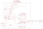
new_lia_low_res.png
 

Hi,

I´m not sure I understood you right.

I talk about voltage path and current path. With both I meant "measurement" paths.

To calculate "Z" you need to know U and I. (For LCRZ you additionallly need phase shift)

Your lower path represents "U" across the DUT.
But the upper path - you call it: "U across the current limiting resistors"...is what I meant with current path. It tells you (you measure U acrosss a KNOWN resistance) the current through the DUT.

So your system should work.

****
In your upper measurement path you have amplifiers. I recommend to use the very same circuit in the lower path (voltage across DUT). As equal as possible.
This should copensate a lot of errors: A delay (or phase shift) in the upper path should be equal to the delay in the lower path...

******
Maybe start with designing of one part of your application: Signal generation. See how it works, see where are the difficulties and optimize it.
Then try to control amplitude (voltage or current) ...

Klaus
 

Hello.

Yeah I get that you couldn't understand, I started writing something and before I eve came half way through my thoughts I found my self very confused and couldn't even recall what I had begun to think about.

But now with a more clear head I do understand what you mean.

I feel I should take your advice but I always find my self trying to(or feeling forced to) get through the design as far as I can so that I can produce a PCB and test many things, all due to economics.

But as I have switched from the AD9954 to the AD9854 I have a AD9954 laying around and the DDS structure is said to be very similar, so I think it might be a good idea for me to produce a PCB with the power supply(s), XMEGA µC, Ad9954 and perhaps a part of the DDS output stage so that I can at least go get through the very basic of controlling a DDS and such.

Darn it, I don't know what's wrong but something is up with me, or my medication because just as in my last post I now find my self really confused and I really can't comprehend much of anything.

I'll return when this whatever it is has passed.
 

I just found out(for the 1000nd time) that phase shift in an amplifier varies over frequency so the idea of compensating the phase shift in software doesn't appear valid, not in a system at this level anywy.

Many commercial LIA store the phase shift vs frequency curve in their software and hence it is not a big deal.

I agree that makes a system (any system) for that matter unnecessarily complex...
 

Hello again.

I would like to ask what you think of my solution for the manipulation of the sine-wave, I don't know what it is that is bugging me but I don't like it.

I would have liked to enable adjustments with digital potentiometers or DACs rather than switching large number of resistors as in the schematic below:
help.png

I know that the current sensing is omitted here, and I just realized that the ADG1606 will surely not be able to handle ±1A...
I also need to add a DAC to a opamp in order to adjust the DC-bias, it was a few weeks ago now but the last time I sat down with LTspice to see what I can do with a DAC connected to different nodes of a opamp with some gain, and for some reason I have gotten it into my head that a DAC should be able to adjust the gain of an opamp but all I could do was to shift the output up/down from the 0V line. Injecting a negative voltage resulted in a positive output DC-bias and injecting a positive voltage resulted in a negative output DC-bias which I have no use for.

I cannot LTspice up a circuit to check if I can connect the opamp output to a DACs Vref pin and then drive the inverting input from the DAC output but it looks to me as that could possibly be used as a PGA, the problem is that my opamp output will swing below and above 0V and as far as I know there are no DACs that can manage that through 1 single Vref pin.
 

Many DACs can be used in a multiplying respectively PGA configuration, e.g. most R-2R ladder DACs. Circuit examples can be found in datasheets.

I remember you previously specified 1 MHz signal frequency for your DDS design. The class B buffer with slow OP won't work well even at 1 kHz.
 
  • Like
Reactions: David_

    David_

    Points: 2
    Helpful Answer Positive Rating
Hi,

Why the second OPAMP?
Don´t under-estimate the capacitance of the analog switches.
Don´t under-estimate the gain erros of OPAM circuits at higher frequencies. (And: a resistor is not an "ideal" resistor anymore. A trace isn´t an "ideal" connection anymore..)

In your circuit there is only the DUT_voltage measurement. I strongly recommend to additionally use a DUT_current measurement.

Klaus
 
  • Like
Reactions: David_

    David_

    Points: 2
    Helpful Answer Positive Rating
It would seem I have some more things to think of and make changes than I thought.

The second opamp was original introduced simply to make things easier in my thoughts, but I have thought to use it to introduce a DC-bias... wait that won't work, I want to be able to introduce a DC-bias that is higher than what the switches is capable of managing.

But can you think of a better way to implement switchable resistors?
would I get more more less parasitics if I used a MOSFET for each resistor, or a BJT?
I guess the switches datasheet should answer that for me, I'll check it out.

I will think about that and finish the schematic so all things are included and then I'll return.

Oh and just to say, the opamps specified in the schematic is just a random opamp chosen for it's schematic symbol, I have yet to select a opamp(s) to use.
If I chose a appropriate opamp would that class B buffer work then?
Would it be better if I biased the transistors properly, I know that there are circuits that looks in principal like the one I have in the schematic only there are some added resistors/diodes/transistors, what the gain of that is I don't quite know.

Regards
 

Hi,

your class B buffer won´t work at all. There is a mistake in your schematic. Both emitters should be connected together.

Other circuits with rsistors, diodes, transistors:
I guess (because I don´t see) they are an improvement according distortion and thermal stability.

Klaus
 
  • Like
Reactions: David_

    David_

    Points: 2
    Helpful Answer Positive Rating
Maybe start with designing of one part of your application: Signal generation. See how it works, see where are the difficulties and optimize it.
Then try to control amplitude (voltage or current) ...
Klaus

Oh yeah, I forgot about that... I should really get going with producing a PCB for the AD9954(even though I can't use it in this design I will use it to get familiar with DDS ICs since I don't own any AD9854 which I can use in this project.
Then at the same time I might as well put a µC on the PCB to ensure that I have understood how to connect and use my programmer in bare bone mcu project.
 

There is a mistake in your schematic. Both emitters should be connected together.
oops. Apparently I did see what I wanted to see. There's always another schematic bug.

If I chose a appropriate opamp would that class B buffer work then?
For MHz output signal, you'll get strong crossover distortions even with a GHz OP. Must use class AB buffer.
 
  • Like
Reactions: David_

    David_

    Points: 2
    Helpful Answer Positive Rating
I have looked a little at the ADG1606 datasheet and some N-channel MOSFET datasheets and it would appear as if MOSFETs input capacitance is quite a bit larger than anything found in the switches, although the MOSFETs I have looked at is designed for high speed SMPS switching.

But is a MOSFET even an option for me in this situation, depending on the type of MOSFET(P-/N-channel) the gate voltage needs to be ether positive or negative to switch the device on, that is positive or negative relative to the source voltage right, but what if I have a sine-wave without any DC-bias.

That might not matter since if I have a gate voltage that is 10V and the sine-wave swings from +5 to -5 then it is always positive and all might be well as long as the gate voltage stays within it's maximum allowed voltage while the sine-wave is at it's most negative.

But if I asked you, by what device capable of switching on/off something would you expect to experience the least parasitics?

Or is parasitics in the signal path something I can calibrate out?

Isn't that what the Open/Short calibration routine is for? Not that I know how it is preformed but at least I know it's possible if I am right that is.

I would be perfectly happy with a multiplexer like ADG1606 if it where not for the fact that I don't believe I will find one such multiplexer that can manage 1A of current, considering that my design was supposed to be able to deliver +-1A current the switching of resistor is starting to look harder than I had hoped.

I am trying to create a LTspice circuit switching resistors with MOSFETa and with BJTs to see if I can see any difference that way, it is an experiment in itself to see what difference I can or cannot discern.
 

Status
Not open for further replies.

Part and Inventory Search

Welcome to EDABoard.com

Sponsor

Back
Top