Continue to Site

Welcome to EDAboard.com

Welcome to our site! EDAboard.com is an international Electronics Discussion Forum focused on EDA software, circuits, schematics, books, theory, papers, asic, pld, 8051, DSP, Network, RF, Analog Design, PCB, Service Manuals... and a whole lot more! To participate you need to register. Registration is free. Click here to register now.

[SOLVED] Layout Capacitor for High Value

Status
Not open for further replies.

kiwi101

Newbie level 6
Joined
Apr 23, 2015
Messages
12
Helped
0
Reputation
0
Reaction score
0
Trophy points
1
Activity points
69
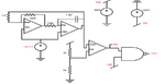
Hey guys I need to make a 22pF Capacitor layout in Cadence and this is the only link I have so Im really confused at how to make a HUGE capacitor with a small area. Please guys guide me
**broken link removed**
 

You found a nice tutorial. What else, exactly, do you need?

What's your process? Which layers do you want to use for the cap? Can you use a MOSCAP? May one terminal be connected to GND?
 

SO I guess I didn't really understand how they got the measuremements for the poly and elec layers in that tutorial

I found another tutorial which walks me through all the steps, but I feel like their is a difference between both tutorials i.e. they are for 2 different processes so which one should I be using?
https://web.engr.oregonstate.edu/~moon/ece423/cadence/example2.html

This is what I am trying to implement.

- - - Updated - - -

Also, my process is the 0.5 micron
 

Attachments

  • Circuit.png
    Circuit.png
    38.1 KB · Views: 74
Last edited:

SO I guess I didn't really understand how they got the measuremements for the poly and elec layers in that tutorial

C = ε0εr * A/t

ε0 = 8.854e-06 pF/µm
εr = 3.9 (for SiO2)
A = cap-area [µm]2
t = thickness of dielectricum [µm] (usually SiO2)

I found another tutorial which walks me through all the steps, but I feel like their is a difference between both tutorials i.e. they are for 2 different processes so which one should I be using?
https://web.engr.oregonstate.edu/~moon/ece423/cadence/example2.html

Also, my process is the 0.5 micron

Also a good tutorial. Does your process offer a MIMCAP option? If not, you have to use different layers.

This is what I am trying to implement.
Now do you need 22pF or 1.5pF ?
 

So I need a 22pF capacitor (sorry about the confusion) so my process does not offer a MIMCAP option
So I guess I will go with the first tutorial
Now even if I follow the first tutorial my l value = 2.75 x 10e-11
Which is very small
So how do I implement that?
 

For a 0.5µm process with double poly option you have a specific capacitance of 0.9fF/(µm)², so you'd need an area A = 22000/0.9 = 24444(µm)² or a square cap of 156*156(µm)² - which is huge!

You could use a MOSCAP, which - for a 0.5µm process with tox=13.5nm - has a specific capacitance of 2.56fF/(µm)². With that, your 22pF cap would need an area A = 22000/2.56 = 8594(µm)² or a square cap of 93*93(µm)² - which is still huge, but perhaps feasible.

A MOSCAP has a voltage-dependent capacity, and for the a.m. specific capacitance it needs a voltage difference of > |Vth|.

It's probably worth to think twice if you really need such a big capacitance. Perhaps you can decrease it by more design ideation?
 

For an analog filter a MOS cap is probably a poor option due to nonlinearity. But at the same time you should never really need capacitances larger than 1pF, it's better to increase R instead so you end up with the same transfer function.
 

Thanks guys
I got it
 

Status
Not open for further replies.

Part and Inventory Search

Welcome to EDABoard.com

Sponsor

Back
Top