Continue to Site

Welcome to EDAboard.com

Welcome to our site! EDAboard.com is an international Electronics Discussion Forum focused on EDA software, circuits, schematics, books, theory, papers, asic, pld, 8051, DSP, Network, RF, Analog Design, PCB, Service Manuals... and a whole lot more! To participate you need to register. Registration is free. Click here to register now.

Klayout simulation issue

salmon_lemon

Newbie
Joined
Jun 3, 2023
Messages
5
Helped
0
Reputation
0
Reaction score
0
Trophy points
1
Activity points
33
I am trying to replicate Figure A of https://www.nature.com/articles/s41566-023-01193-1 using KLayout tool.

What step did I miss other than "export netlist" ?
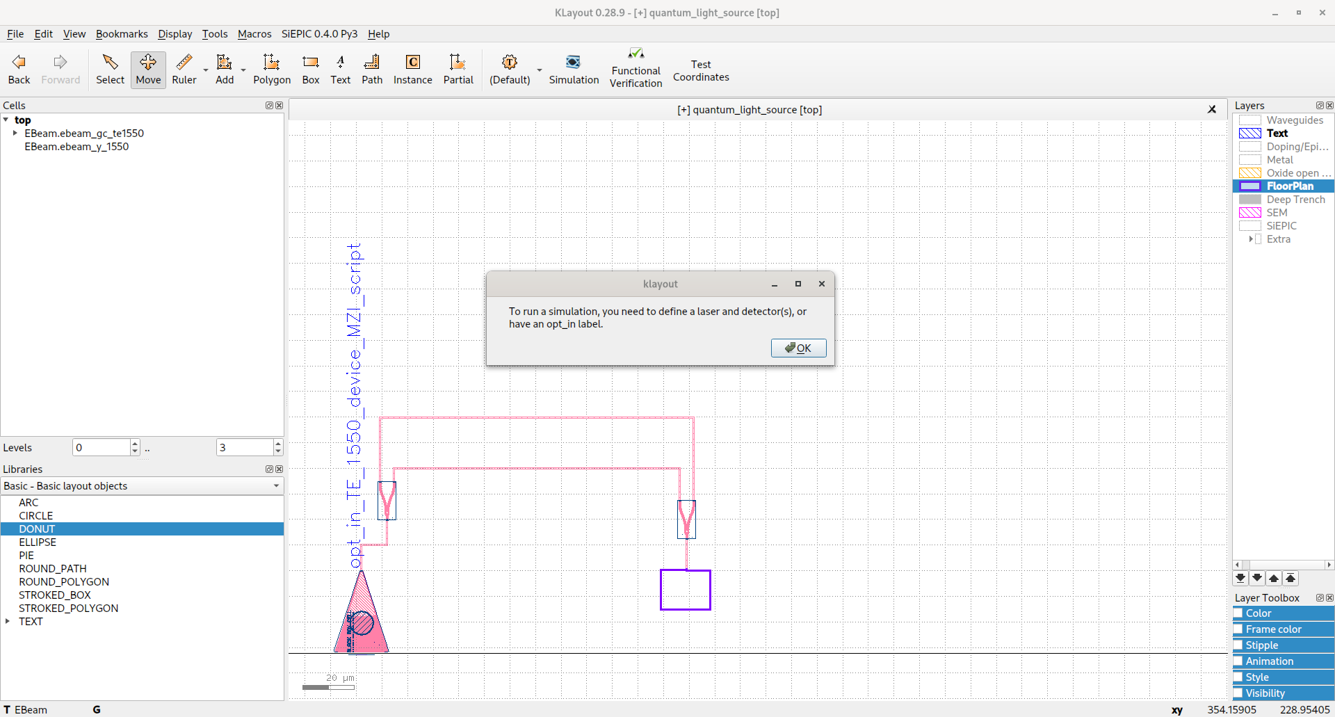
Screenshot from 2023-06-12 13-32-11.png
 
You know that klayout is a layout, not a schematics tool, right?

To get a layout to extract as a netlist may be "doable" but require
a lot of groundwork (recognition / extraction rules) to create such
a netlist. And that picture seems to lack a lot of connections that
a functioning SPICE netlist would want (power, inputs, outputs).
The simulation complaint window is one I have not seen (as I
use Xschem for schematics, which is a more appropriate tool when
layout details do not drive simulation - though photonics in the
present day, is not really that). Whether you can, by heroic effort,
make klayout cough up a layout-geometry-driven netlist / models,
I couldn't predict. But I can predict it will be a long hard slog with
a lot of questionable data to turn into formulas for models and
values.

There is no Figure A in the linked article. What you show looks
not much like Figure 1. So that's another thing.

It seems there -is- (contrib) support for photonics layout and in
the linked page for "Klayout" (which seems to be a side branch).
There are sub-links for "how to use" all that "stuff". You may find
very few mentors for this "path less taken" and the actual klayout
forum would probably be a much better place to ask (try with
better material to work from). The SiEpic (?) folks may also have
a useful forum (or failing that, their git page might have some
discussion / feedback you could use).
 
Thanks for your tips. I will definitely reach out to Klayout and/or SiEpic people/forum/mailing list if they are active and responsive.

Note: I meant Figure 1A

By the way, I had converted the path for sagnac mirror to waveguide by using "W" shortcut keystroke.
Warning: One of the waveguide segments has insufficient length to accommodate the desired bend radius.
Not sure how to get around this above quoted warning though.
Nevertheless, I have updated sagnac mirror waveguide in the latest github commit.

sagnac_mirror_waveguide.png


As for the netlist issue, see the following:

No netlist available. Cannot run simulation.
/home/phung/.klayout/salt/siepic_tools/python/SiEPIC/netlist.py:48
/home/phung/.klayout/salt/siepic_tools/python/SiEPIC/netlist.py:38
/home/phung/.klayout/salt/siepic_tools/python/SiEPIC/opics_netlist_sim.py:41
/home/phung/.klayout/salt/siepic_tools/pymacros/Keybindings/Simulation/circuit_simulation OPICS.lym:7
 

LaTeX Commands Quick-Menu:

Similar threads

Part and Inventory Search

Welcome to EDABoard.com

Sponsor

Back
Top