andrelux
Junior Member level 1

- Joined
- Sep 18, 2008
- Messages
- 17
- Helped
- 0
- Reputation
- 0
- Reaction score
- 0
- Trophy points
- 1,281
- Activity points
- 1,405
Hi All,
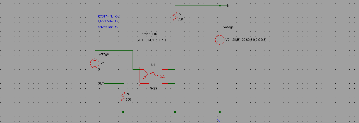
I am looking for a very reliable design using isolation barrier for voltage feedback on a industrial battery charger.
Normal operating voltage to monitor ranges from 120 V (Battery low) to 180 V (battery fully charged)
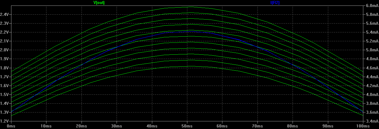
I guess that I do not need any sophisticated compensation on the optocoupler because of the stability of the load.
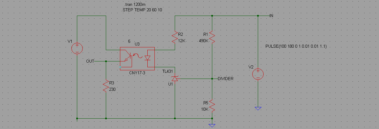
Architecture of the charger is classic:
230 VAC Mains-> Rectifier and Caps -> 325 VDC bus -> 20 KHz IGBT Full Bridge -> HF Trafo -> Secondary rectifier -> Output Filter
PWM chip should be a TL494. Control strategy is Voltage mode, with a external overcurrent trigger.
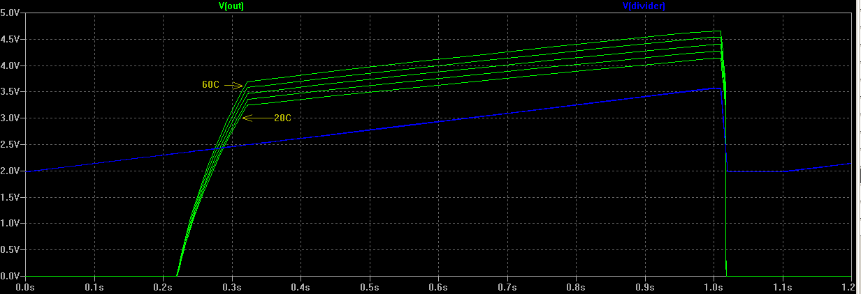
Feedback excursion from an opto output should vary from 1 to 2 volts range when output varies from 120 to 180 V.
What do you think of this first draft:

I Have also included the LTSpice model.
Thanks for your help.
I am looking for a very reliable design using isolation barrier for voltage feedback on a industrial battery charger.
Normal operating voltage to monitor ranges from 120 V (Battery low) to 180 V (battery fully charged)
I guess that I do not need any sophisticated compensation on the optocoupler because of the stability of the load.
Architecture of the charger is classic:
230 VAC Mains-> Rectifier and Caps -> 325 VDC bus -> 20 KHz IGBT Full Bridge -> HF Trafo -> Secondary rectifier -> Output Filter
PWM chip should be a TL494. Control strategy is Voltage mode, with a external overcurrent trigger.
Feedback excursion from an opto output should vary from 1 to 2 volts range when output varies from 120 to 180 V.
What do you think of this first draft:
I Have also included the LTSpice model.
Thanks for your help.