Continue to Site

Welcome to EDAboard.com

Welcome to our site! EDAboard.com is an international Electronics Discussion Forum focused on EDA software, circuits, schematics, books, theory, papers, asic, pld, 8051, DSP, Network, RF, Analog Design, PCB, Service Manuals... and a whole lot more! To participate you need to register. Registration is free. Click here to register now.

Isolated devices - where to connect N-tub?

Status
Not open for further replies.

kb81

Newbie level 4
Joined
Sep 6, 2007
Messages
6
Helped
0
Reputation
0
Reaction score
0
Trophy points
1,281
Activity points
1,324
Suppose I have a bunch of isolated PMOS/NMOS devices inside and NWELL/NBL tub. What voltage should the NWELL/NBL tub be connected to? So far I have usually seen the tub connected to the highest voltage seen by devices in the tub. For example if the device is an isolated inverter connected between PGND and PVDD then the tub is connected to PVDD. But what is the disadvantage of connecting the tub to PGND? After-all the enclosed P+ inside the tub is also at PGND so the diode between the NTUB and the enclosed P well will not be forward biased - correct?

Would appreciate your inputs - thank you!
 

... what is the disadvantage of connecting the tub to PGND?
The electrically active nodes source & drain would be forward biased - no MOS transistor action possible.

After-all the enclosed P+ inside the tub is also at PGND so the diode between the NTUB and the enclosed P well will not be forward biased - correct?
That's right: 2 regions at the same potential aren't biased at all. If there is an enclosed P+ (ring) in an NWELL, it is connected to the source of a MOSFET (or to the collector of a PNP BJT). Even a P+ area or ring inside the NWELL and connected to GND wouldn't matter, because it would be reverse biased (as you wrote). The active transistor regions, however, must never be forward biased in respect to the NWELL, that's why the latter must always have a higher (= more positive) potential.
 

The electrically active nodes source & drain would be forward biased - no MOS transistor action possible

That is not true because the source and drain say of a NMOS inside the NTUB will still have a higher or equal potential to the P region enclosed inside the isolation NTUB. Correct?


The active transistor regions, however, must never be forward biased in respect to the NWELL, that's why the latter must always have a higher (= more positive) potential.

This is my question though - the isolating NTUB is not in direct contact with the active regions of any transistor. There is always the enclosed P region inside the NTUB, which is kept at PGND. So what forward bias exactly are we concerned about? [/QUOTE]
 

The construction of your NTUB - NWELL isn't clear for me. For further discussion pls. show a cross-section!
 

Hi Erikl,

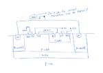
Attached is a cross section isotub.png

My question is asked on the picture. The PSUB of the chip is connected to AGND (analog ground).
 

High kb81,

I didn't think of a triple-well process like your isotub image above (or the following below), because you didn't mention it before, sorry!


Of course you can connect the isolation tub (deep N-well) to PGND in this case, but by that you depredate the chance of much better isolation if you'd connect it to PVDD ! In the latter case (PVDD connection), a much wider inside and outside space-charge region is created, which collects straying electrons (and repels holes) from both sides, so achieves a much better isolation between the inner P-well and the outside P-sub (substrate) region.
 

Thanks for the response Erikl. Yes I should have mentioned triple well. And indeed yes the space charge region would be wider if the Ntub is connected to a higher voltage.
 

Status
Not open for further replies.

Part and Inventory Search

Welcome to EDABoard.com

Sponsor

Back
Top