Continue to Site

Welcome to EDAboard.com

Welcome to our site! EDAboard.com is an international Electronics Discussion Forum focused on EDA software, circuits, schematics, books, theory, papers, asic, pld, 8051, DSP, Network, RF, Analog Design, PCB, Service Manuals... and a whole lot more! To participate you need to register. Registration is free. Click here to register now.

Is this a good way to place dummy transistors ?

Status
Not open for further replies.

DoYouLinux

Advanced Member level 4
Joined
Sep 26, 2007
Messages
113
Helped
3
Reputation
6
Reaction score
5
Trophy points
1,298
Activity points
2,152
Hi all,

I am designing a 7 GHz ring oscillator and looking for a good practical way to place dummy transistors for each functional transistor.

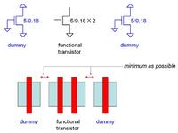
As shown in the attached figure, for example, in case that I have a functional transistor having a size of 10/0.18 (5/0.18 with 2 fingers) and I would like to add dummy transistors to this functional transistor. Is it correct that I just add two independent (isolated) transistors, each having a size of 5/0.18 and all terminals are grounded (for NMOS) to both sides of the functional transistor ? Then, as shown in the layout, the distance between the dummy transistors and the functional transistors have to kept as small as possible, right ?

Thank you very much in advance,

DYLinux

 
More dummy, more matching, more guard ring.

yap you're right. For nmos, connecting all the terminals to ground. For pmos, connecting all the terminals to vdd in order to shut down the transistor.
 

A better approach would to be one continuous diffusion. For your functional transistor, let the area between the two gates be the drain and the area outside the two gates be the source. Connect your source of the functional transistor to gnd as well as the gates and drain of the dummies.
 
Thank you very much, Shaq and mince :D

What I am still wondering is that:

1) In case that I connect the dummy transistors to each side of a functional transistor (sharing the source/drain region), what about the gate ? Is it necessary to connect the gate of the dummy to the gate of the functional transistor ? Or can I just ground the gate (for NMOS) to deactivate the dummy ?

2) Since my design is working at very high frequency, so if possible, I do not want to attach the dummy transistors to the functional transistor (trying to avoid further loading the functional transistor with more parasitic capacitance). Due to this concern, can I still place the dummy transistors separately from the function transistor and ground all terminals as shown in the figure ? To avoid the edge effect, I agree that sharing the drain/source region would be better, but concerning the contribution of capacitance from the dummy devices, would it also be possible to use separate dummy devices to avoid this contribution ?

Thank you very much to you all again

DYLinux
 

1) You wouldn't connect the dummy gate to the other gate. You would ground it.

2) The additional capacitance from adding a dummy shouldn't be very much since you are sharing the source diffusion.
 
try to consider these in laying out sensitive devices:

-- same width for all xsistors and dummies
-- it is not necessary to for the dummy device gate length to be equal to the gate
length of the transistor
-- gate to gate spacing of transistors including the dummies should be the same
-- DO NOT connect the dummies to the transistor specially to its drain because these
affect the AC characteristic of the device ( for Diff amp)
-- drain to source orientation must be the same. dont share source and drain if your
area permits

regards

Added after 5 minutes:

mince said:
A better approach would to be one continuous diffusion. For your functional transistor, let the area between the two gates be the drain and the area outside the two gates be the source. Connect your source of the functional transistor to gnd as well as the gates and drain of the dummies.

this is possible if the dummy element is in the schematic; otherwise there will be LVS errors...
 
It is essential to have spacing between all the poly same....so if you are sharing the source and drain terminal of functional transistor, you should also share dummy with functional mos. If not possible to share then go for multipliers instead of fingering. and u can connect all the terminals of the dummy to VSS or source. avoid connecting it to drain.
 

Status
Not open for further replies.

Part and Inventory Search

Welcome to EDABoard.com

Sponsor

Back
Top