Continue to Site

Welcome to EDAboard.com

Welcome to our site! EDAboard.com is an international Electronics Discussion Forum focused on EDA software, circuits, schematics, books, theory, papers, asic, pld, 8051, DSP, Network, RF, Analog Design, PCB, Service Manuals... and a whole lot more! To participate you need to register. Registration is free. Click here to register now.

Is there a chip which includes a D FlipFlop and also a DELAYED Clock?

Status
Not open for further replies.

Lironsh

Newbie level 5
Joined
Oct 19, 2013
Messages
10
Helped
0
Reputation
0
Reaction score
0
Trophy points
1
Activity points
100
Hello all,
Is there a chip which includes a D FlipFlop and also a DELAYED Clock? I want to press a button and at the same time turn on an LED on the output.
My solution so far is to use a 74x175 DFF and two inverters in series from 4069 chip for the clock so i can get my t_setup on time in one press.

Anyone knows one chip for that?

Thanks,
Liron.
 

Could you post here the waveform explaining timing of these signals ?


+++
 

Sure.
I want it to act as a latch, but I haven't seen any chip that has the delay included inside yet.


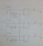
20131020_004319.jpg
 
Last edited:

The function you want achieve is called "monostable".
Once a programable timing is required, you need some circuit able to work with a RC network.

Take a look on LM555.


+++
 

Since the delay is in nano seconds, a simple RC could be added between the switch and the clock pin to ensure that, at the rising edge of the clock, D is high and stable.
But I think it is a bit more complicated than this. A mechnical switch may generates several pulses at transition from off to on and vice versa (during about 50ms for example). I suggest adding a small diode (as 1N4148) to reset (discharge) the capacitor at the leading edges of the switch positive pulses during the transition time.

The resistor between the switch terminal and the clock pin could be 4K7 and the capacitor between the clock pin and the ground 100pF.
The anode of the diode is connected to the clock pin and its cathode to the switch terminal (the diode is in parallel with 4K7).

Note:
The clock pin has an internal capacitance (I assume we are talking about CMOS digital series) so perhaps 4K7 could be increased to 47K so that the 100pF could be removed.
 
Last edited:

...a simple RC could be added between the switch and the clock pin.....adding a small diode (as 1N4148) to reset (discharge) the capacitor

In fact, this could avoid the need to use an integrated circuit to perform this task.
However, coupling impedance of this network to D_FF may be properly dimensioned, in case to be not an CMOS input, but TTL.

+++
 

However, coupling impedance of this network to D_FF may be properly dimensioned, in case to be not an CMOS input, but TTL.

You are right. It is not practical using an RC circuit at a TTL input as a delay network.
 

With some presumptions
- the "button" would output a clear digital pulse (it actually doesn't)
- you are implementing the said delay (that's the easiest part)
what's the operation of the circuit?
It switches the FF on, but never off. So what is it good for?

There are in fact many ways to process a button in digital logic, but I think we need to know the complete problem.

Some circuit elements that are generally helpful for bouncing buttons:
- RC filters to supress contact bounce
- schmitt trigger gates to convert filtered signals to clear digital signals
- RS flip flops, monoflops, toggle circuits
 

Thank you all for the professional replies.
I attached a clearer pic of my issue.
In order to focus on my issue in the circuit I connected LEDs (with tact switches). So it is now a basic Switch, i want to have 3 LEDs turned on and stay on in the Q output accordingly to the button pressed (there is a use of a simple pull-down resistor instead of a filter). every time a different switch is pressed, it will clear the other LEDs.

I understand the options such as adding a capacitor, but i am trying to avoid adding more parts to my circuit. in fact, I want to remove part from my board, all I'm seeking for is a one DFF chip that has enough delay on the CLK so i could save the second chip (inverter) that is used only for buffer. but i couldn't find this chip, my challenge is to remove the "inverter" chip without adding other components.

anyone think it's possible somehow or should i go and produce my own chip? (i'll have to start saving some $$ for the real estate on the wafers...)

Switch.jpg


Liron.
 

D-FF of which series?
Are you connecting 3 outputs of the 3 second inverters together to trigger the 3 clocks?
 

Correct. in this way i can clear the input of the others whenever i press on one button, and i make only my specific LED turned on.

When the clock rise, the others have ground in "D" input from the pull-down resistor.
 

Are you connecting 3 outputs of the 3 second inverters together to trigger the 3 clocks?
This won't work, there must be OR logic.

I'm sure that the intended functionality can be better implemented with RS latches, using cross coupled NAND or NOR gates.
 

On last schematic you posted, is still missing the R-C network, or some other circuit able to achieve required debounce.
As said by KerimF, magnitude order of switch contact glitch (mili-sec) is much higher than delay generated by some inverters(nano-sec).

Why don´t you consider about to use an extreme simple 6 pins microcontroler ?


+++
 

Regarding the MCU, it's the simplest solution for me, but I was trying to design my circuit with passive components, without involving MCU (not afraid of MCU, just trying to get a solution in this way).

What RC Network to achieve my required debounce? I do get my results with my current configuration, my buffer gives me enough delay for DFF Setup time, but also short enough to have it in one "button press" that is pressed by a human's finger. as i wrote, i don't want to add more components, my goal is to remove the Buffer chip.

I will still look for a DFF with different characteristics (such as longer "T_Hold time" built-in inside the DFF). i'm pretty sure the chip is out there and i just don't find its name.
 

It is good that you were able connecting 3 ouputs to clock together 3 ICs.
When all switches are open, these three inverter outputs are low (no problem).
When one switch is pressed only one output of the 3 will try to be high while the other two connected to it have to be low. In your circuit, it seems this high output is not affected at all by the other two low outputs and does its job as if it is alone by clocking the 3 D-FFs. Did I understand your circuit well?
 

Correct. This is what I meant that by Turn on an LED accordingly to the button switch. I tested it and it works perfectly (The theory proved itself again).

So yes, you understood the circuit.
 

I wish I know the IC names of your inverters and D-FF. Unless the outputs are open collector/drain (or tri-state and one of them is made active), I cannot see myself connecting them to a single node. This is why I asked you the names of ICs ;)
 

If you accept inversion between in- and outputs, a single IC-package, either 74HC10 (3xNAND3) or 74HC27 (3xNOR3) can achieve the intended function.
 

Or even connect the 3 outputs through 3 diodes ( common kathode ), preventing high level output short circuit to low level outputs.
Even with diode drop voltage, output still will stay on a valid logic region.

+++
 

Yes Andre, but I am surprised that on his schematic there are neither diodes at the outputs nor a pull-down resistor for the 3 clock inputs.
 

Status
Not open for further replies.

Part and Inventory Search

Welcome to EDABoard.com

Sponsor

Back
Top