Continue to Site

Welcome to EDAboard.com

Welcome to our site! EDAboard.com is an international Electronics Discussion Forum focused on EDA software, circuits, schematics, books, theory, papers, asic, pld, 8051, DSP, Network, RF, Analog Design, PCB, Service Manuals... and a whole lot more! To participate you need to register. Registration is free. Click here to register now.

IO date bit width of delta-sigma in PLL

Status
Not open for further replies.

shadow_cuk

Newbie level 3
Joined
Nov 16, 2009
Messages
4
Helped
0
Reputation
0
Reaction score
0
Trophy points
1,281
Activity points
1,304
2_1299579523.jpg

2_1299579638.jpg


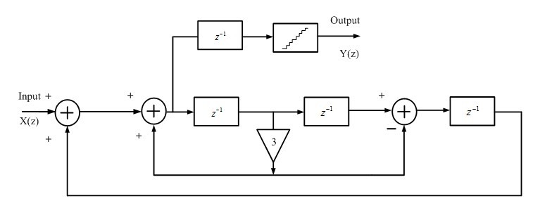
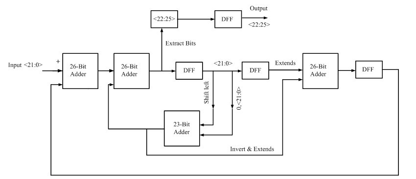
this DSM is used in a fractional-N PLL,but i dont know how to translate the signal flow graph to real circuit like the second picture,another question is how to determine the bit width of the input and output data,thx!
 

Shadow-cuk,

The diagram at the top is the idealised form where the signals flowing between the blocks are nebulous and not defined, they could be serial data parrellel data or some combination of both it does not matter as it is not relevant to the functioning.

However the second diagram is not idealised and is a minmalised practical overview of an implemented system. In this system it is showing the data moving between the blocks as "data widths" thus "<21:0>" means bits 21 through to bit zero thus the input is 21 bits wide.

In the upper diagram the circles with crosses in are adders and on the diagram below their input size is given such as "26bit adder". In the upper diagram you see a triangle with a 3 in it this effectivly means "multiply by three" in the lower diagram this is done by a left shift (mul by 2) added to the number so giving a result of 2+1 or 3.

In the upper diagram the z^-1 blocks are time delay elements of one clock period which in the lower diag are shown as DFF for D type Flip Flops.

I hope that gives you suficient info to get your head around it.

lurchman

thanks for your answers,now i understand that z^-1 is a DFF block and 1-z^-1 equals accumulator after reviewing the singal process textbook, so far i still don't understand how to calculate the bit width exactly,the input bit width k can be deduced by minimum frequency precision which is determined by fref*(1/2^k),fref is the referfence frequency of the PLL,but what about the output,why extract <25:22>,why 4bit,i see that there are some DSM output 1bit quantized signal,what's the difference?

best regards
 

Status
Not open for further replies.

Similar threads

Part and Inventory Search

Welcome to EDABoard.com

Sponsor

Back
Top