Continue to Site

Welcome to EDAboard.com

Welcome to our site! EDAboard.com is an international Electronics Discussion Forum focused on EDA software, circuits, schematics, books, theory, papers, asic, pld, 8051, DSP, Network, RF, Analog Design, PCB, Service Manuals... and a whole lot more! To participate you need to register. Registration is free. Click here to register now.

Interference in low noise amplifier

Status
Not open for further replies.

koushikr_in

Member level 2
Joined
Aug 18, 2004
Messages
42
Helped
1
Reputation
2
Reaction score
1
Trophy points
1,288
Activity points
356
Hi,

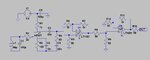
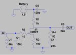
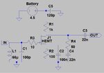
I am designing low noise amplifier using HEMT ATF34143. The frequency of operation is around 1-2 MHz. The HEMT is followed by two stages of opamp (OPA847) (Gain=2000).

I would like to measure the total output noise of my amplifiers. I don't see any interference when I measure the noise of the opamp stage alone. When the HEMT is connected at the input of opamp, I see a 50 Hz modulation of my noise signal. Why?

A battery is used as power supply for the amplifiers. Measurements are dne with an ADC at a sampling rate of 20 MHz.

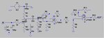
The ouput waveforms are attached.
 

Attachments

  • NoiseFullchain.bmp
    946.7 KB · Views: 94
  • HemtonlyNoise_timedom.bmp
    946.7 KB · Views: 87
  • OpAmpNoise_timedom.bmp
    946.7 KB · Views: 85

That's one heck of a choice of transistor to amplify 2MHz! Are you sure it isn't oscillating? Showing the circuit would be useful.

Keith
 

Hi,

The reason for using HEMT is because of low temperature operability (cryogenic environment) of the device. It is stable. I have checked the spectrum. No signs of oscillation. The operating point is Vds=160 mV, Ids=4 mA
 

Attachments

  • Full_Chain.jpg
    Full_Chain.jpg
    30 KB · Views: 111

As an ignorant question: Do you know, if the noise figure of HEMT is also low at 1 MHz, in other words, what's theie 1/f corner frequency? It's not stated in the datasheet.

I also remember, that other devices can be used at cryogenic temperatures. But if low frequency noise is O.K., a HEMT should work.

The interference looks like some signal being picked up from the enviroment, obviously from a mains operated instrument. So the question goes back to you.
 

Hi,

I don't know the noise figure of HEMT at 2 MHz. The measurements that I had uploaded were taken at room temperature. I don't really understand why there is no interference when I measure opamp. Interference is only present when HEMT is included in the circuit.

Is the HEMT acting like a mixer? Is there a way to eliminate this?

Only the computer is powered my mains and the digitizer card is in the pci slot of computer

-RK
 

It is difficult to tell where the input is on your circuit - for example at R3/C1 junction or the other end of C1? Also there are floating nets which I assume should be grounded e.g. R2/C2/C4 junction. I suggest you look at the power supply to the HEMT.

Keith.
 

Is the HEMT acting like a mixer? Is there a way to eliminate this?
Of course, if suitable RF are allowed to enter the circuit. But as Keith mentioned, you should show a correct circuit first. To determine possible interference pathes, we would need to see a layout photo as well. E.g., if the supply battery is connected by a cable, I don't think that a 100 pF capacitor will achieve sufficient filtering against RF pick up.
 

I had a problem with 50Hz mains pickup when using low noise op-amps some years ago (medical EEG design)
In the end I had to put bandpass filters in each channel. (simple RC did the trick)
Once you've got the circuit cleaned up if you find you still have a problem
give that a go.

jack
 

When I test my low noise amplifiers, I see the exact same noise patterns that you do in your second image. It's EMI radiated from the environment. However, it's not a 50-60Hz sine wave, but rather bursts of noise modulated at the line frequency (or sometimes twice the line frequency). Again, same thing I saw. In my case, turning off any nearby fluorescent lights helped reduce it a lot. There was also a particular computer in the lab with an incredibly noisy power supply which would cause it too. So you need to either hunt down the source of the EMI and kill it, or shield the whole preamplifier in a copper box.
 

Hi,

I am attaching the correct circuit diagram and layout files. The amplifier (common source amp) is mounted inside an aluminium box (see image) and everything is enclosed by a faraday cage to minimize interference.

Should I have extra capacitor for power supply bypass? How do I minimize interference?

-RK
 

Attachments

  • Full_Chain.jpg
    Full_Chain.jpg
    47.9 KB · Views: 98
  • HEMT layout.jpg
    HEMT layout.jpg
    38.5 KB · Views: 106
  • Image0366.jpg
    Image0366.jpg
    61.5 KB · Views: 102

A hand calculation says, that the transistor will operate at effectively no Vds with your dimensioning, so the performance will be at least poor, the voltage gain would be around -12 dB a 5 mA/25 ohm load even with sufficient Vds, in this case the circuit may be still a reasonable impedance converter, of course.

But the point hasn't to do with interferences. Yes, I would add effective filtering of the supply voltage.

Regarding possible oscillations, plugging a termination resistor to the input would reliably stop it. But the said bias situation makes it unlikely anyway.

Also, does removal of the preamp power stop the interferences?

Regarding localization of interference sources, I fully agree with mtwieg.
 

Removal of preamp power stops interference. Interference is present when it is powered on. Also having a input termination resistor (across the input LC tank circuit) doesnot make any difference. The interference is still present.

The choice of the operating point takes into consideration the maximum allowable heat dissipation in the cryogenic environment. My main requirement is low noise operation of the device.
 

The choice of the operating point takes into consideration the maximum allowable heat dissipation in the cryogenic environment.
Yes, I know. But ohms law should be considered, too. The datasheet has no specification for 4 mA Id, but it's absolutely clear, that a transistor can't amplify in ohmic region. Did you calculate and measure the operation point of the circuit?

To place the transistor in active operation, you only have to reduce the drain resistor value. This won't increase the drain current much, otherwise a source resistor of e.g. 120 or 150 ohm should be used. But Vds should be at least 0.5 or 1V.
 

I had done some measurements where the transistor saturates at Vds> 100 mV. My Vds is 170 mV approx. Similar characteristics were observed in the cryogenic environment as well.

Reg power supply filtering, do RF beads help? I am also planning to add 100 nF parallel to the 100 pF in the power supply line.
 

I had done some measurements where the transistor saturates at Vds> 100 mV. My Vds is 170 mV approx.
Why do you set 170 mV when you have 4.5V supply? But if the intended output voltage is very low and the achieved gain sufficient... I can't imagine that the noise performance will be good, too. Having Vds that low also considerably "improves" the amplifier's ability to act as a mixer for RF interfernces at low levels.

Reg power supply filtering, do RF beads help? I am also planning to add 100 nF parallel to the 100 pF in the power supply line.
As long as you can't identify the interfering source it's almost guessing, but these measures are reasonable in any case.
 

66 db of voltage gain--you are going to need shielding or it WILL oscillate. Make the two op amps on a seperate board and put a good faraday shield around them all. If you have a narrowband signal, it might be good to insert an appropriate filter (either lowpass, highpass, or bandpass) somewhere in the chain to kill the total gain at frequencies you are not interested in--it makes the shielding job easier if you only have to deal with one frequency instead of a broad band of frequencies.
 

Hi,

The circuit of common source amplifier is attached. ckt4 is amplifier with no source bypass capacitor. In ckt5 the source bypass capacitor c2 is added. The ckt5 shows some strange output (50 Hz modulation present). The amplifier is biased with a battery. The measurements are the output noise of the amplifier. (no input connected to amplifier).

What is the role of the source bypass capacitor? The only reason I want to use the capacitor is to increase the low frequency gain.
Please help me out.
 

Attachments

  • ckt4.jpg
    ckt4.jpg
    36.6 KB · Views: 99
  • ckt4_time.bmp
    946.7 KB · Views: 80
  • ckt5.jpg
    ckt5.jpg
    38.9 KB · Views: 98
  • ckt5_time.bmp
    946.7 KB · Views: 77

What is the role of the source bypass capacitor? The only reason I want to use the capacitor is to increase the low frequency gain.
Yes, that's a reasonable assumption. If omitting/placing the capacitor is the only change between both measurements, you have proved, that the interferences are somehow demodulated or generated by the preamp. High frequency oscillations of the preamp would be an explanation, but I rather guess, that the interfering signal is picked up by the power supply wiring and demodulated due to the unsuitable transistor bias point.
 

Status
Not open for further replies.

Similar threads

Part and Inventory Search

Welcome to EDABoard.com

Sponsor

Back
Top