Continue to Site

Welcome to EDAboard.com

Welcome to our site! EDAboard.com is an international Electronics Discussion Forum focused on EDA software, circuits, schematics, books, theory, papers, asic, pld, 8051, DSP, Network, RF, Analog Design, PCB, Service Manuals... and a whole lot more! To participate you need to register. Registration is free. Click here to register now.

Input offset voltage of 2 stage opamp.

Status
Not open for further replies.

saqib.shah06

Junior Member level 2
Joined
Nov 29, 2009
Messages
23
Helped
0
Reputation
0
Reaction score
1
Trophy points
1,281
Location
India
Activity points
1,518
Hi Everyone,
I am trying to simulate a two stage opamp (NMOS input). I am not concerned about random offset (for now I am only trying to fix systematic offset). I have the following question:

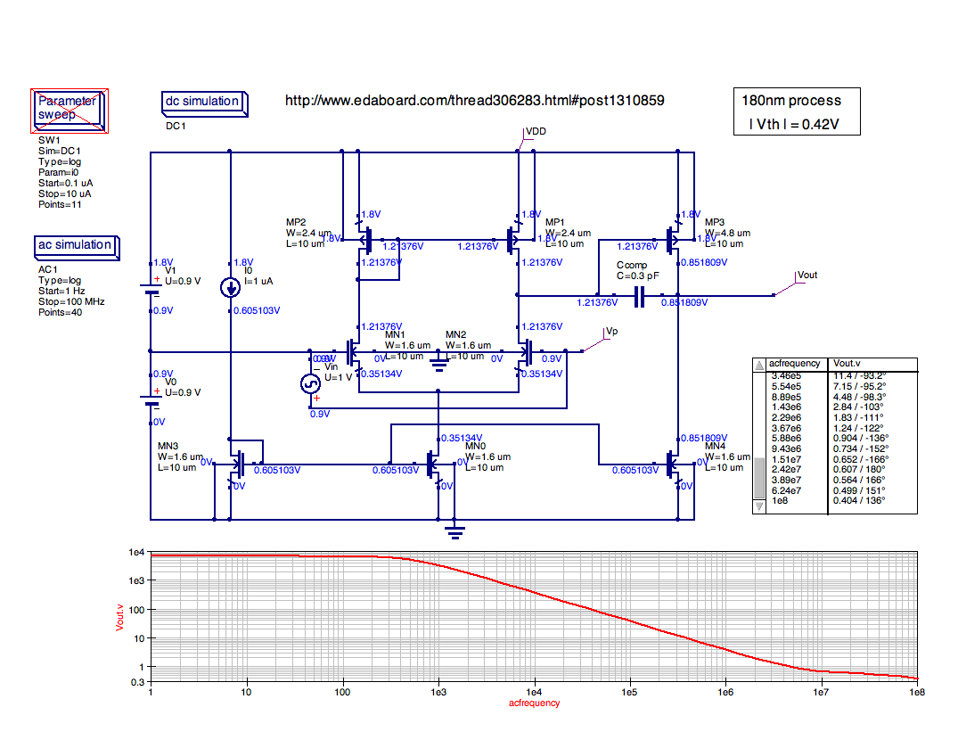
If I size the MOSFETs "perfectly" so that the bias current is exactly split between the input pair, should I still get a systematic offset? I have attached a figure in the post for your reference. I have tied sizing the MOSFETs according to what the text book says. When I apply a CM voltage of 900 mV, my output transistor (NMOS load - MN4) still remains in triode region - could anybody please explain why this happening?

Thanks for any replies.
 

Attachments

  • Screenshot-5.png
    Screenshot-5.png
    66.1 KB · Views: 128

For balanced output, MN4 must be half the area of MN0.
 

For balanced output, MN4 must be half the area of MN0.

Thank you for your reply, caould you please explain a little as to why MN4 wouldve to be half the area of MN0?
 

Thank you once again. Here is the logic I used:

Lets assume MN0 is carrying 1uA. Since MN4 is sized similar, it'll also carry 1uA. The 1uA splits between MP1 and MP2 which get 500nA each. Since MP3 (output PMOS) gets all of the 1uA, it should be sized at twice the width of MP1/MP2 to have the same overdrive voltage. (as you can see mp1/2 are sized at W=2.4u and mp3 is sized at w=4.8u).

Am I right or did I make a mistake somewhere in there?
 

Yes, I didn't noticed double width of MP3.

You should monitor operation points of all transistors and also determine the actual input offset.

There will be still a certain inbalance due to different Vds.
 

First of all You should simulating this OPAMP in closed loop, i.e. as bufer. To minimalize systematic offset You also should have the same finger width in current mirrors.
 

When I apply a CM voltage of 900 mV, my output transistor (NMOS load - MN4) still remains in triode region

What are the threshold voltages of your process? Is it a 180nm process?

For our (low Vth, fast) 180nm process your design shows quite reasonable operating points:


What are the threshold voltages of your process? Is it a 180nm process?

For our (low Vth, fast) 180nm process your design shows quite reasonable operating points:


Thank you for your reply. This is a CSM .35um process. Threshold is around 400mV. I tried by reducing the current in the output stage to 1/2 and changing the output PMOS sizing to half of the original as well (4.8u/2 = 2.4u). In this case the circuit works fine and all the transistors are in saturation - Any ideas?
 

Status
Not open for further replies.

Similar threads

Part and Inventory Search

Welcome to EDABoard.com

Sponsor

Back
Top