Continue to Site

Welcome to EDAboard.com

Welcome to our site! EDAboard.com is an international Electronics Discussion Forum focused on EDA software, circuits, schematics, books, theory, papers, asic, pld, 8051, DSP, Network, RF, Analog Design, PCB, Service Manuals... and a whole lot more! To participate you need to register. Registration is free. Click here to register now.

Double supply Two-stage OPAMP

noor84

Member level 5
Joined
Dec 27, 2017
Messages
90
Helped
0
Reputation
0
Reaction score
0
Trophy points
6
Activity points
688
Hi all,

I am designing A two-stage OPAMP with double supply (vdd=2.5, vss=-2.5) using Cadence (Virtuoso),

The question is, in the simulation to find the output offset voltage, for example, should the DC voltage be 2.5V or 5V as shown in the attached picture), and why?
The same question is for all other measurements required such as common mode gain, CMRR, etc.

If I use one power supply, should the DC voltage be (1/2) vdd? and why?

Thanks in advance.
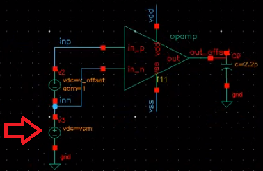
1695081506689.png

--- Updated ---

Continue to the question,

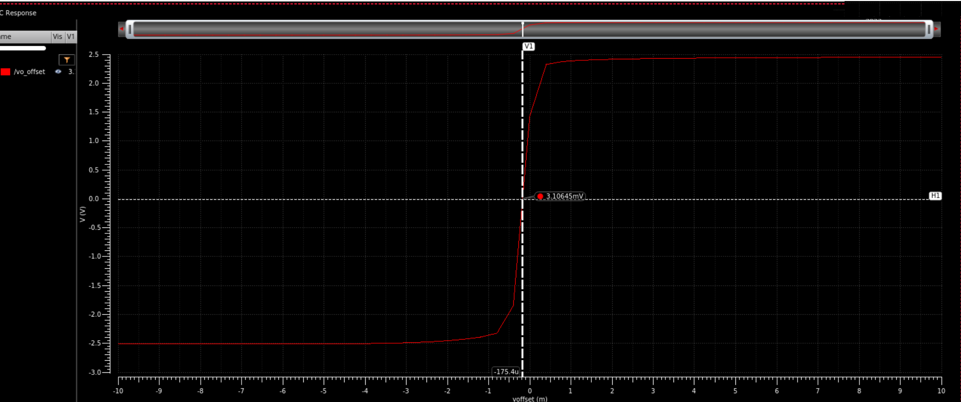
The result shown below is when the VCM(DC)=2.5V, then the Voltage offset is (175 uV), is that correct?

(This figure is maximize)
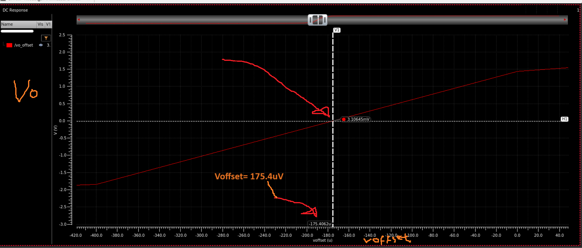
1695082582417.png


(The figure without Maximize)
1695082764256.png
 
Last edited:
When you get to real silicon testing ground (TCOM) referred is
far preferable. Most instruments have fixed range / resolution
and do scaling, so operating at a DC offset eats LSBs (or many)
in the instrument. Using active test hardware can help accuracy
and repeatability. Links have been shown and attachments made,
before.

You can make 2.5V or anything within useful common mode
range you like, a "virtual ground" for your signal processing.
You will have consequences probably. Ground is ground. Your
virtual girlfriend is not your girlfriend.

The tools you use don't matter to this. The questions are about
art and practice, learning the things that are not in books (though
app notes are your friend).
 
You have an Opamp with Bi-Polar supply of +/- 2.5V.

This would mean that the reasonable input common mode range for your opamp would be -2.5V to +2.5V. (Assuming it is rail to rail input)
Similarly, assuming it has a rail to rail output, , the reasonable output common mode range would be slightly lesser, say about -2.4V to +2.4V.

Now you would want to measure your offset somewhere within your operating range. Not someplace close to one of the supply rails since that would probably not be the usual operating point for the OpAmp.

As a part of convention, we usually go for (Vdd-Vss)/2 as a common mode point where one can do the measurement of the offset.
I have seen datasheets where they have measured at (Vdd-Vss)/4 as well.
The above voltages are comfortably in the operating range of the Opamp and will give a realistic result.

PS, the worst case might not be necessarily be at (Vdd-Vss)/2 or /4 or anything. That might depend on the process corner and other parameters. It might not be practical to find out the Worst case point for each PVT corner since it might lead to a large number of simulations. So the conventions help in that way.
 
It makes sense to have a bipolar supply for a circuit where you have bipolar AC in/out. That's when it seems natural to think in terms of a 0V centerline. And it seems natural to think zero in, zero out. Even the 741 op amp can be adjusted to give zero out for zero in... with a bipolar supply.

However when you use a single-ended supply you must continually be aware of a midway reference voltage. And though you input zero V to your op amp it doesn't necessarily give you zero V output. For instance the 741 output is never closer than 2V to the lower supply rail. That's the reason early advice about op amp IC's told us to use a bipolar supply.
 
Thank you for your comments,

Then, the measurement of input offset voltage value depends on the Common mode range, and the way of the measurement, the values in the previous pictures for the VCM and others are correct!! right? (No error in the connection) and the values.
 
You have an Opamp with Bi-Polar supply of +/- 2.5V.

This would mean that the reasonable input common mode range for your opamp would be -2.5V to +2.5V. (Assuming it is rail to rail input)
Similarly, assuming it has a rail to rail output, , the reasonable output common mode range would be slightly lesser, say about -2.4V to +2.4V.

Now you would want to measure your offset somewhere within your operating range. Not someplace close to one of the supply rails since that would probably not be the usual operating point for the OpAmp.

As a part of convention, we usually go for (Vdd-Vss)/2 as a common mode point where one can do the measurement of the offset.
I have seen datasheets where they have measured at (Vdd-Vss)/4 as well.
The above voltages are comfortably in the operating range of the Opamp and will give a realistic result.

PS, the worst case might not be necessarily be at (Vdd-Vss)/2 or /4 or anything. That might depend on the process corner and other parameters. It might not be practical to find out the Worst case point for each PVT corner since it might lead to a large number of simulations. So the conventions help in that way.
Hi nitish5,

regarding your comment(As a part of convention, we usually go for (Vdd-Vss)/2 as a common mode point where one can do the measurement of the offset.)

the common mode point should be the midpoint (vdd+vss)/2 or (vdd-vss)/2?

Regards
 
the common mode point should be the midpoint (vdd+vss)/2 or (vdd-vss)/2?
Whatever gives the actual midpoint according to your math. Following the notation in post #1 (vdd=2.5, vss=-2.5) the midpoint is obviously 0.
 
Hi,
I am designing A two-stage OPAMP with double supply (vdd=2.5, vss=-2.5) using Cadence (Virtuoso),

when measuring the value of the Diff gain and CM gain measurement of the OP-AMP to measure the CMRR, is the common mode voltage in the input (vdd+vss/2)?
if yes this mean the DC voltage for both inputs should be 0V? is that right?

in case for the single supply voltage (Vdd=1.8 , vss=0), the DC voltage for both inputs should be 900mV is that right?

see the attached picture.
Thanks


1695553051089.png

--- Updated ---

Whatever gives the actual midpoint according to your math. Following the notation in post #1 (vdd=2.5, vss=-2.5) the midpoint is obviously 0.
HI FvM, thanks for your reply,

Then, the VCM (common mode voltage for both inputs is 0V for (vdd2.5, vss-2.5) and 0.9 for (vdd=1.8, vss= 0) is that right?
 
Last edited:
Hi,

* wrong parenthesis. It should be Vmid = (Vdd + Vss) / 2
* never minus (-) , always plus (+)

Klaus
Thanks KlausST,

is the configuration of measuring the open loop gain and the common mode gain correct as in the last picture?
 
Hi,

I have no clear answer to your question, that's the reason why I didn't write it.

Thus I can tell just about my worries and ideas:

There are several methods how to measure CMRR.
Opamp manufacturers provide application notes on how they do it (and why).
I just did an internet search on this topic. They provide schematics, mathematics and background information.

But I've not seen the schematic you use. Where is your schematic from? Is it a valid method to measure CMRR at all?

I'm not sure whether you want CMRR measurement in real life or in simulation.
If simulation: Does it give meaningful results at all? Because bad CMRR is mainly caused by production errors (like resistor mismatch).

Klaus
 
Measuring common and differential mode gain in open loop is more a theoretical setup than a practical method, because it requires offsets to be manually trimmed. It may not work at all with high gain OPs. Therefore practical measurement circuits are mostly using closes loop setup. You'd know if you read OP application notes.
 

LaTeX Commands Quick-Menu:

Similar threads

Part and Inventory Search

Welcome to EDABoard.com

Sponsor

Back
Top