Continue to Site

Welcome to EDAboard.com

Welcome to our site! EDAboard.com is an international Electronics Discussion Forum focused on EDA software, circuits, schematics, books, theory, papers, asic, pld, 8051, DSP, Network, RF, Analog Design, PCB, Service Manuals... and a whole lot more! To participate you need to register. Registration is free. Click here to register now.

Input and Output Capacitance of NMOS

Status
Not open for further replies.

rshrivas

Newbie level 4
Joined
Jan 15, 2011
Messages
7
Helped
0
Reputation
0
Reaction score
0
Trophy points
1,281
Activity points
1,338
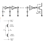
I am designing a NOT gate chain to drive a NMOS switch. The NOT gate is made up of one PMOS between the vdd and o/p and a NMOS between op and gnd..

I need to find out the value of input and output capacitance of the NOT gate..

The strategy I am using is to find Cgg and Cdd for both the NMOS and PMOS and then adding Cggpmos + Cggnmos and using it as input capacitance.. Similarly using Cdd of PMOS and NMOS together and adding them together to get the output cap...

Kindly let me know if my strategy is correct....
 

Hey my friend!
Without your schematic . how can i help you????!!!!!!!!!

I have attached my the circuit diagram...I am using cadence virtuoso and I need to find the input n output cap for the NOT gate schematic...
 

Attachments

  • Citcuit Diagram.png
    Citcuit Diagram.png
    22.9 KB · Views: 168

the equivalent capacitance is better found using simulation (this is how std cell characterization tools do it)

if you want to have an approximation from model parameters you have to take into account the miller effect which adds to the pure gate capacitance, the result is
Cin = 3/2 (Coxp +Coxn)
Cout = Coxp +Coxn

See Baker, 2nd ed, p. 337
 

hi,
virtuoso tells you these values. just simulate and print or annotate the component parameters of the transistor you want. a lot of parameters will be listed and you can search for the related capacitances. I guess, the input capacitance of an inverter is Cnmos + Cpmos. Cnmos = Cox,n + Cgd,n + Cdb,n + Cgs,n. Cpmos is the same as nmos.
Virtuoso can provide you with these values, but if you want to calculate them by hand, it is a complicated process and it doesn't promise an accurate result.

This book explains the capacitance issues very well in one of the first chapters: CMOS Digital Integrated Circuits Analysis & Design by Sung-Mo (Steve) Kang and Yusuf Leblebici
 

Dear Friend
Hi
my mean is internal circuit. because in ac equivalent circuits , you can see : cP.( Capacitance of base to emitter or gate to source or gate to emitter junction. ) its capacitance is depend on the transistors. you should analyse your equivalent circuit. if you give your accurate circuit (with value of your components and part number of your transistors , i can do calculations of your circuit and get back its calculation to you.
Though , As you wish.
Wish you the best
Goldsmith
 

Dear dgnani,

How to define the Cox. As my understanding, Cox is the constant parameter of a transistor. Can the simulator calculate is for me? If yes, I use the Spectre, which print parameter is refer to Cox.

Thanks,

TDF

the equivalent capacitance is better found using simulation (this is how std cell characterization tools do it)

if you want to have an approximation from model parameters you have to take into account the miller effect which adds to the pure gate capacitance, the result is
Cin = 3/2 (Coxp +Coxn)
Cout = Coxp +Coxn

See Baker, 2nd ed, p. 337


---------- Post added at 06:25 ---------- Previous post was at 04:49 ----------

Hi,

I also search on the Baker book, and found that the Cox depends on the epsilon_0 (e0) and epsilon_r (er). e0 is a constant parameter and er is 3.97 for SiO2. Thus, the er is 3.97 for all the generic SiO2 process, can anyone confirm it for me.

Rgs,

TDF
 

Dear dgnani,

How to define the Cox. As my understanding, Cox is the constant parameter of a transistor. Can the simulator calculate is for me? If yes, I use the Spectre, which print parameter is refer to Cox.

Thanks,

TDF

In spectre not all models use cox as a model parameter in addition cox in models is a specific capacitance (capacitance per unit area) which is not the case for the expressions I quoted to calculate an approximation of gate cap in digital gates - those are straight gate capacitances. Most likely you need to use tox (the gate oxide thickness) to calculate it as eps0*epsr/tox then multiply the result by the gate area. There are additional subtleties which might not be worth going into given that these are just approximations

I also search on the Baker book, and found that the Cox depends on the epsilon_0 (e0) and epsilon_r (er). e0 is a constant parameter and er is 3.97 for SiO2. Thus, the er is 3.97 for all the generic SiO2 process, can anyone confirm it for me.

Rgs,

TDF
You might want to confirm with the PDK design manual or the SPICE model themselves which value was used as it is common for different foundries to use different values
 

e0 is a constant parameter and er is 3.97 for SiO2. Thus, the er is 3.97 for all the generic SiO2 process, can anyone confirm it for me.
Yes, you're right, see my former answer here (at the top).
Before, I gave you a wrong value, sorry. I've deleted this wrong posting.
 

in spectre epsrox defaults to 3.9 (not 3.97) but in general different foundries will use different numbers. They can even use different numbers for gate oxide and interlayer dielectric oxide so you can verify your case either directly in the SPICE models or in the SPICE model manual. In any case any number around 3.9 won't make much of a difference...
 

The capacitance as seen from the gate terminal varies with voltage.
Your Qgg includes both the integrated Cgs(Vgs)*dVgs and the output
Miller capacitance integrated Cds*Vds, Cdg*Vdg and these can be
the dominant term in a high voltage device (owing to large V).

I'm not sure what you intend to do with this information but my
preference is to drive the gate stop-to-stop, use a cccs referenced
to the driving source and stuff its current onto a (say) 1pF cap.
Qgg=V*1pF there, and Cgg=Qgg/(Vmax-Vmin). Similarly drive the
drain (of an "off" FET) and pick off the drain charge.

Now when switching there is also a shoot-through current which
likely dominates the switching charge as seen from the supply
and output terminals. The single-transistor method will not
tell you about that, but presents an ideal lower bound to
charge per cycle.
 

Status
Not open for further replies.

Part and Inventory Search

Welcome to EDABoard.com

Sponsor

Back
Top