phanikiran
Junior Member level 2
[moved] influence of LAMBDA, current and Vds on rds of MOSFET in saturation regio
In MOS FET, specifically while designing amplifiers ( a simple Diode Load Differential amplifier) UGB will decides the gm of input differential pair width and slew rate decides the current, swing decides the Load PMOS widths. Here my problem is . if i go for higher slew rates current will increase and the LAMBDA parameter is drastically varying which varies rds of PMOS load finally it effecting my gain.
If i choose low currents ,input differential pair taking higher widths to give the reuired gm finally it also affecting gain.
I found rds is the main parameter which is not the value i expected.
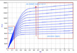
I did experiment by varying Vds , and i got required rds for larger vds( depth of saturation is very high ex 1v)
how can i expect rds for a specific vds , how LAMBDA influences for currents (becauseit varying very drastically with high curretns?
