umery2k75
Advanced Member level 1
via orcad layout
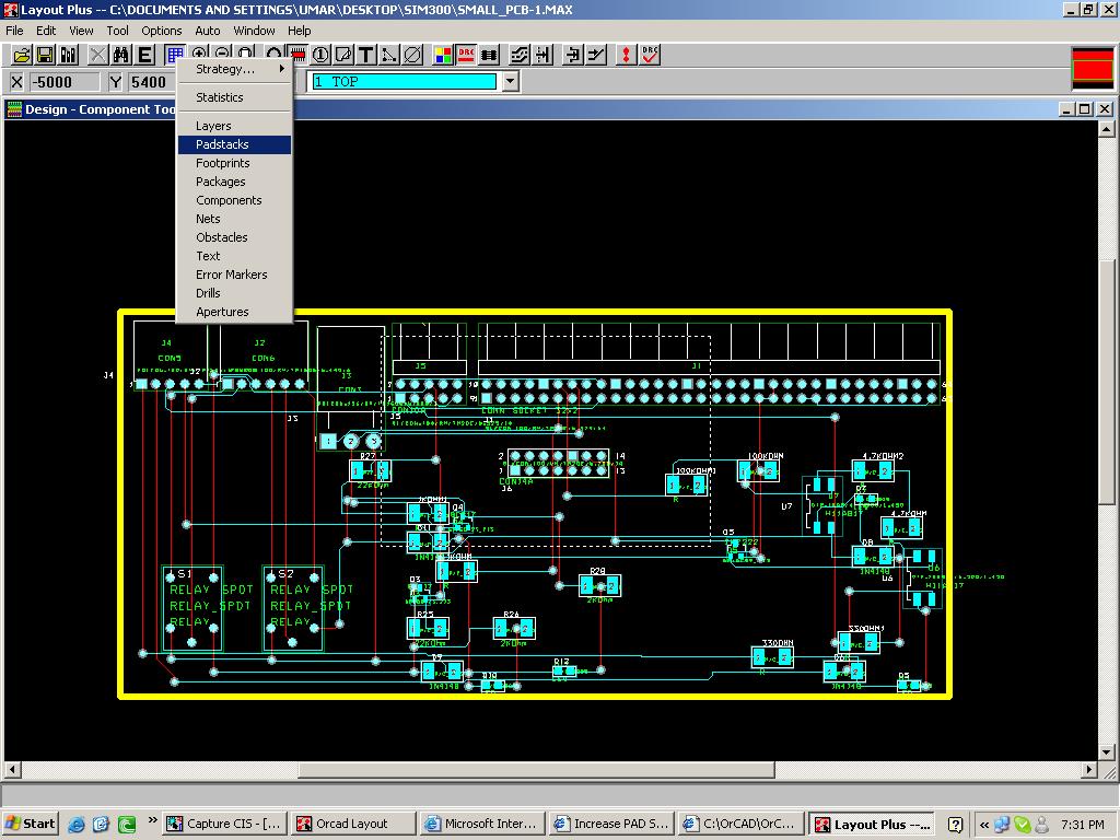
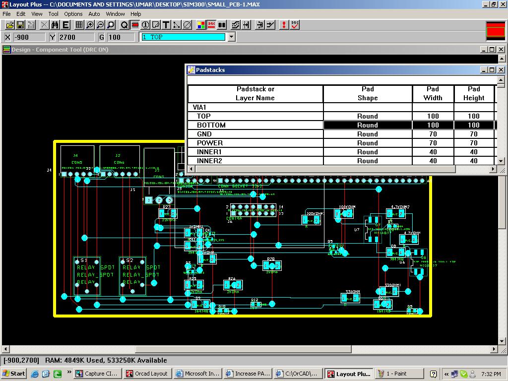
I can't find any place in Orcad 10 Layout/Layout Plus to increase the size of the VIA. I actually want to increase the size of the VIA, because I want to make the 2 sided PCB using the toner transfer method and the via size is small, it's almost the same size as the least size of my drill.So when there will be very little pad left on the copper sheet, after doing the drilling, it will becomes almost impossible to solder the VIA with wire.As I will be placing the jumper wire connection between TOP and BOTTOM and the jumper will be inside the VIA or HOLE.I am doing testing, so I have to make many PCBs during testing and that's why I am making them at home, if the design was final, I would have sent them to PCB manufacturer, but making alternation every time and giving them to manufacturer makes very much delay, as I don't know how many times I have to make the alteration and the design is SMD.
When I searched the internet about this,I found basic tutorials, which I already knew.
Added after 5 minutes:
I found it out
Added after 12 minutes: