Aani
Newbie level 4
Hi,
Iam using the I2c communication protocol considering FPGA as I2C master and TMP513 as I2C slave device.
But during the process of this I2C communication, I am able to write the data to slave device and get the slave acknowledgement back. But during read operation, the slave is giving out the data as 0x0000 to the master (FPGA) for any internal register access.
The A0 pin has been grounded in the hardware, so the 7-bit slave address given is 1011100.
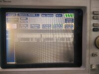
And also I do see the device returning the value 0x0000 on the Logic Analyzer, to master (FPGA) instead of non-zero value, during the read operation performed for one of the Internal Register (i.e., Device ID register (Address = 0x1F/FF) with data 0x23FF).
Please help me out where am I doing wrong for the data is being read as 0x0000 all the time.
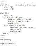
SDA line conditions in code:
SDA <= SDA_OUT when SDA_OE = '1' else 'Z';
SDA_IN <= SDA when SDA_OE = '0' else '0';
Thank You.
Iam using the I2c communication protocol considering FPGA as I2C master and TMP513 as I2C slave device.
But during the process of this I2C communication, I am able to write the data to slave device and get the slave acknowledgement back. But during read operation, the slave is giving out the data as 0x0000 to the master (FPGA) for any internal register access.
The A0 pin has been grounded in the hardware, so the 7-bit slave address given is 1011100.
And also I do see the device returning the value 0x0000 on the Logic Analyzer, to master (FPGA) instead of non-zero value, during the read operation performed for one of the Internal Register (i.e., Device ID register (Address = 0x1F/FF) with data 0x23FF).
Please help me out where am I doing wrong for the data is being read as 0x0000 all the time.
SDA line conditions in code:
SDA <= SDA_OUT when SDA_OE = '1' else 'Z';
SDA_IN <= SDA when SDA_OE = '0' else '0';
Thank You.
Last edited: