Continue to Site

Welcome to EDAboard.com

Welcome to our site! EDAboard.com is an international Electronics Discussion Forum focused on EDA software, circuits, schematics, books, theory, papers, asic, pld, 8051, DSP, Network, RF, Analog Design, PCB, Service Manuals... and a whole lot more! To participate you need to register. Registration is free. Click here to register now.

I/O pad simulation : calculation of drive current ,pull-up and pull-down resistances

Status
Not open for further replies.

dileep4111

Junior Member level 1
Joined
Dec 30, 2012
Messages
16
Helped
0
Reputation
0
Reaction score
0
Trophy points
1,281
Visit site
Activity points
1,372
What is drive current for a PAD and how to decide drive current for I/O PAD while doing characterization.Also how to calculate the pull-up and pull-down resistance for I/O pad cells.

Thanks
 

What is drive current for a PAD
The current which can be driven by the output buffer of the pad.

how to decide drive current for I/O PAD while doing characterization.
While doing characterization you measure - you can't decide on your results (just if they are reasonable).

how to calculate the pull-up and pull-down resistance for I/O pad cells.
Depends on requirements (customer's or yours).
 
How should i characterize the drive current of pad. Currently i am using Spectre tool from cadance.
thank you
 

Which type of pad? Analog or digital? Output only or I/O pad?
 

It is I/O PAD

Again: Analog or digital? Provide its schematic!

BTW: Slowly I'm running out of endurance, if you're not even willing to provide the info necessary to be able to respond to your questions!
 
Last edited:

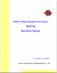
So why don't you simply have a look into the respective TSMC Standard I/O Lib Data Book? E.g. this one: TSMC_0,18u_Std_IO_lib_cover.gif
If you rightfully got the schematic and/or layout of the cell, you'd have access to it, too. There you can find the drive capabilities:
Pls. notice the correlation between a part of the cell name and its drive capability!


If you want to simulate: Enable the output, set a logic input voltage, measure the output current, either in short circuit mode, or into a known output load up to your requirement. Repeat this for the other logic input voltage.

Hope this helps!
 
Status
Not open for further replies.

Part and Inventory Search

Welcome to EDABoard.com

Sponsor

Back
Top