Continue to Site

Welcome to EDAboard.com

Welcome to our site! EDAboard.com is an international Electronics Discussion Forum focused on EDA software, circuits, schematics, books, theory, papers, asic, pld, 8051, DSP, Network, RF, Analog Design, PCB, Service Manuals... and a whole lot more! To participate you need to register. Registration is free. Click here to register now.

I am nearly get fired becoz of thermal relief

Status
Not open for further replies.

bloke203

Member level 1
Joined
Jan 20, 2010
Messages
33
Helped
2
Reputation
4
Reaction score
2
Trophy points
1,288
Location
UK
Activity points
1,578
Dear All

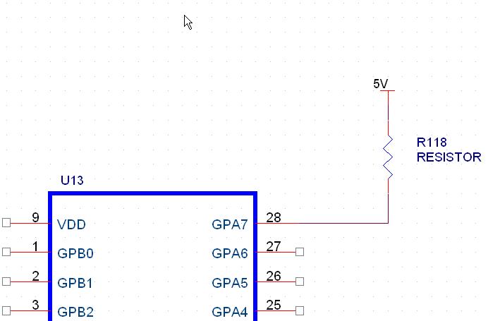
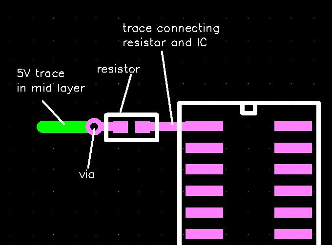
I am really in an awkward position. My employer ask me to place a 1206 package resistor between the 5V track and the pin X to the IC. So I did. We are not using any seperate ground plane and power plane And, we do machine soldering. And there is always a solder mask to the PCB. There was a 0.25mm width of 5V track. I am not been told that how much current is flowing.

The 5V track comes thru the second layer of the PCB board

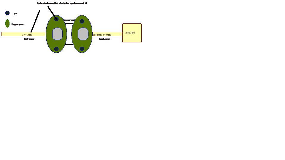
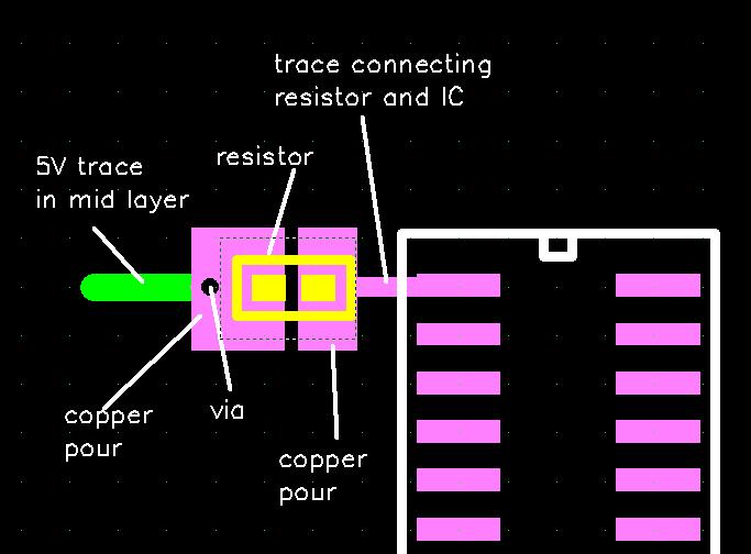
But he is saying that I should have to place a thermal relief around a resistor. If I am right, thermal relief should need a little bit copper around the resistor pads and connect them to the ground (with via hole). If I did then the 5V track and the ground via can make it SHORT circuit.

IF I do it differently like instead of connecting to the ground, if I connect the via to the 5V then I am worried, what would be the purpose of it?

Second, If PCB layout guy not been told how much current is flowing and the width of the track is small then how would the layout guy know to place a thermal relief?

Can anypne help me?

Thanks
 

I'm not sure how far your responsibilities go, or where your expertise fits within a larger organization, but if he just said put this here, and you did, because that's your job, and there is no company guidelines or accepted design principles that you should be using, then shame on him.

Personally, within my responsibilities, if someone said "put this here", my first of 20 or so questions would be "Why?" If you have the responsibility of making sure everything works, and this caused a problem, then shame on you.

The more important things he will / should be looking for is: how did this mistake happen, how can we fix it and how can it be prevented on future projects. If you can help him answer these, without pointing fingers at him, then you should be fine.
 

is thermal relief really needed for a SMD component????
I have heard that we need thermal relief only for thru hole component. This is to help assembly process.


I never used thermal relief for SMDs but for thru holes I am using it.
 
Last edited:

thermal reliefs can be helpful for smd's as well, for the same reasons. without thermal relief, smd's can take longer to reflow when connected to a large plane, and cool much quicker. this may or may not cause a problem, similar to using them on thd's, may or may not make a difference. I personally don't use them on smd's, and very rarely on thd's, unless there are internal plane connections, or we see a problem with solder taking forever to reflow when prototyping.
 

Guys

I like the response of NIKHILRAJ and Jnnewtom. Please sort out my concept. Please answer to my Qs. I really need that.

Thanks
 

You may need to check the max current drawn from PIN X of IC (From datasheet). Then you can calculate the required trace width of 5V power supply (Search in google how to calculate). Once you get the current value, you will know the total power dissipation on resistor. 1206 package can handle up to 1/8 Watt. If you think it is not enough, you may need to increase the size.
When you draw the PCB, you can use the copper plain for 5V power supply to resistor instead of using trace. The copper plain can help to apply enough current and work as thermal relief.
 

form your queris what I got is you need a connection as shown in picture1.But here why we need to bother about ground? thrmal relief and Ground have no relations.
I hope you are placing the IC and pull-up rersistor in top side and you have a 5V copper pour in bottom side. So you just put a 5V via near the Resistor pin and connect it using a trace.here thermal relief has no significanve. for power trace try to use 0.508 mm trace width. in picture2 yellow color represents Top layer and green color bottom side.

regarding the high current trace designer should inform the PCB designer about high current traces


63_1289207892.jpg
 
Thanks Raj for the effort you did to explain me. This is what I am tring to understand that what is the significance of the thermal relief. As you said there is no need of it.

To further explain, There is no 5V plane. It just a 5V track is coming from Mid layer 1 and it need to go to the top layer to make the connection with the resistor pad. I agree with you that I just have to need a 5V via which connect the track from Mid layer to top layer and thats it.

What is happened? He further place a copper pour around the resistor pad and then he connect the copper pour with the 5V via.
What is the signifance of it? I really don't understad the concept. and he is using a 0.25mm thick 5V track.

Thanks
 

Guys

I like the response of NIKHILRAJ and Jnnewtom. Please sort out my concept. Please answer to my Qs. I really need that.

Thanks

There are many things that we need to know to answer your questions. For instance:

If there are no planes, why are thermals being considered? If there is to be a plane, is it significant enough to cause a large temp difference during reflow?
Why are you placing the resistor between the IC pin and +5V?
What is the resistance, and why have you chosen that?

How many layers is your board? If it is only two, this is probably a non-issue, if it is more with a connection through a via to an internal layer, you may want thermals.

Why 1206 SMD? Normally the size is chosen after the current draw is known.

What are the specifics of the input? Input impedance, protection, max V.
Is the resistor for current limiting for schottkies on a <5V device?
What are the max If of the diodes?

If all of these seem normal, you probably don't need any thermals.

These would be a start.

If you cannot answer these types of questions, then the answer to your questions are all "I am unable to determine an answer from the information given"
 

Hi

If there are no planes, why are thermals being considered? If there is to be a plane, is it significant enough to cause a large temp difference during reflow?

Ans:- I said that there is no power lane or ground plane. This is the question I want to know from you. I do not agree at first place that we should place a thermal relief. Are you confirming that if there is no plane that I am right to not place a thermal relief??

Why are you placing the resistor between the IC pin and +5V?

Ans: They want to drop the voltage to 4.3V

What is the resistance, and why have you chosen that?

I do not rem exactly. But it is around 1K

How many layers is your board? If it is only two, this is probably a non-issue, if it is more with a connection through a via to an internal layer, you may want thermals.

Ans: The board consist of 4 layer. The 5V track is coming from mid layer 1 and goes to top layer. In order to do that, we need a 5V via to connect the mid layer and top layer traces.

Why 1206 SMD? Normally the size is chosen after the current draw is known.

Ans: I did not design the circuit. I was asked simply to go to that design and place a resistor 1206 package between so and so.
What are the specifics of the input? Input impedance, protection, max V.
Is the resistor for current limiting for schottkies on a <5V device?
What are the max If of the diodes?

Ans: The Raj has shown up the schematic circuit above. It is more like same thing I was doing.
 

Your fabricator is asking for thermal relief on smd resistor just to avoid dry soldeing because if we make filled copper on smd pad it will act as heat sink and will result in heat dissipation which in turn will cause Solder to dry even before components(In your case resistor 1206) is placed so what will happen is component will not be properly soldered.It is not necessary that it will hapeen with every smd component but it is a possibilityi.e. why thermal relief is provided even on SMD's
What you can do here is claculate or get the current that 5V power supply will draw then you can calculate the track width from any calculator available online (or i generally take 1mm for 1A).
Once you have the track width divide it by no. of spokes you are going to provide on thernal relief (4 spokes generally),so suppose you have claculted the tracl width to be somewhere aroun 4mm so you provide thermal relief with spoke width of 1 mm each.
 

You have no plane, therefore no heat sink, therefore each side of the resistor will reflow approx the same. If the someone is worried about the fact that it is a 1206, you are dropping 0.7V over 1k, so 0.7^2/1000 => 0.00049W, a 1206 is way more than you need.

Solder that monster down and move on.
 

I'm under the impression, that the term thermal relief is used in the original post different from it's common meaning. It's normally designating a thermal isolation of pads from a plane or copper pour. The latest picture is too blurred to shine a light on the problem. So I still didn't exactly understand what your boss wanted (and if it's reasonable or not).

Regarding thermal reliefs (in it's common sense) for SMD parts: I think that most reflow solder processes are heating the PCB as a whole up to the solder temperature. In this situation, thermal reliefs are useless, except for manual rework. We also have an increasing number of designs, that use the PCB as a heatsink for power components in small packages, utilizing exposed pads and thermal vias. They need a complete heating during solder anyway. I also remember manufacturer footprint suggestions for some larger SMD parts, e.g. tantalum capacitors, to use larger pads for reflow layouts, to allow heat transport from the PCB to the part during solder. i don't say, that these considerations apply to any PCB design, but they are valid for most that I know.
 

hi Bloke,
I assume you did the PCB as I shown in image1. But in this case i think you do not need a copper pour there. you could connect it using copper trace(as in image 2). (No issue with circuit functioning in both cases.)

In both cases no need to worry about thermal relief ( hope no special temperature requiremets in your board/).


Last edited:
Thanks FvM and Nikhilraj for your great effort. The Niikhilraj snapshot is the right one. It is now clear to me.
 

I would ask the circuit designer first if he really needs a thermal relief. But usually, the posts above are correct, SMD components seldom need thermal relief, unless it is dropped right in the middle of a plane.
 

Status
Not open for further replies.

Part and Inventory Search

Welcome to EDABoard.com

Sponsor

Back
Top