Continue to Site

Welcome to EDAboard.com

Welcome to our site! EDAboard.com is an international Electronics Discussion Forum focused on EDA software, circuits, schematics, books, theory, papers, asic, pld, 8051, DSP, Network, RF, Analog Design, PCB, Service Manuals... and a whole lot more! To participate you need to register. Registration is free. Click here to register now.

HVIC malfunctioned when DC voltage is larger than 130V.

Status
Not open for further replies.

nealxgs

Newbie level 5
Newbie level 5
Joined
Mar 23, 2006
Messages
8
Helped
1
Reputation
2
Reaction score
1
Trophy points
1,283
Visit site
Activity points
1,341
Dear all,

I designed a Half H bridge by a HVIC switching circuit, but I encountered some problems.

This is my schematic.
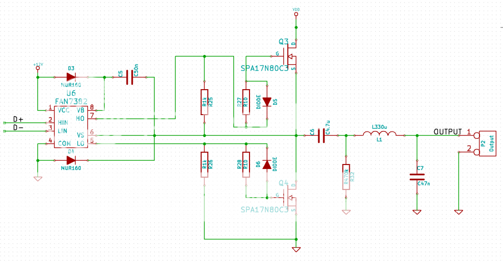
HBridge.png


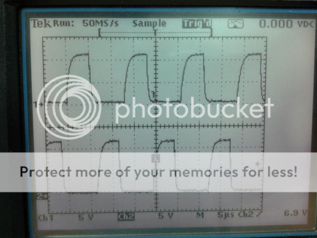
The circuit is working perfectly when I applied the VDD below 100V.

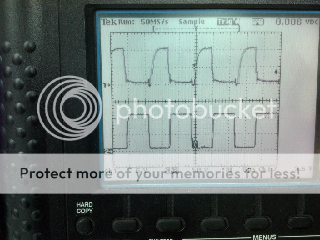
Following is the chart from oscilloscope, for the Vgs of both up-side and low-side MOSFET.
HVIC_GS_Initial.jpg


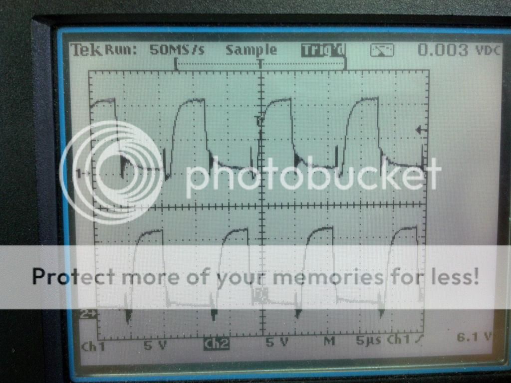
However, when I increase the VDD to 130V, the Vgs start to distort, making me be confused, as below,
HVIC_GS_130V.jpg


when I increase the VDD more, the HVIC malfunctioned and burned.

What should I do to avoid the problem?


the HVIC I have used is NCP5106BPG, from ON-semi, and another one is FAN7382, from Fairchild.

In datasheet, they both can achieve to 600V in VDD, I think 130V is piece of cake for them.


Thanks advance for your patient and reading !
 

I don't see an obvious problem in the schematic. May be a matter of circuit layout.

Can you show the low-side Vds waveform? A photo of the circuit?
 

It is obvious (to me) from the Vgs that tail voltage that the current from Qg begins does not switch off fast enough falling transition.

The gate driver needs a lower resistance driving low on the high side especially to prevent shoot thru failure that you experienced. Both could be improved then your deadband can be reduced.
 

According to post #1, failure of gate driver was observed, I understand that the power transistors are still operational.

I agree that the sinking capability could be improved, but according to waveforms, there's not yet an unintended turn-on due to miller capacitance. The situation may be different at higher bus voltages, but still wouldn't explain why the drivers are destroyed without damaging the output transistors. It's usually no problem to operate gate driver ICs in current limiting, at least not with moderate switching frequency.

The "most popular" way to destroy drivers selectively is massive undershoot of Vs. That's why I want to see the circuit layout.
 

Dear All, thanks for your helping. Now I post the Vgs-Vds for High Side MOSFET and my layout of HVIC.

Vgs-Vds for High Side MOSFET:

VGS_VDS.jpg


The Vds looks well, but when I increase the VDD higher than 130V, the wave start the distort.


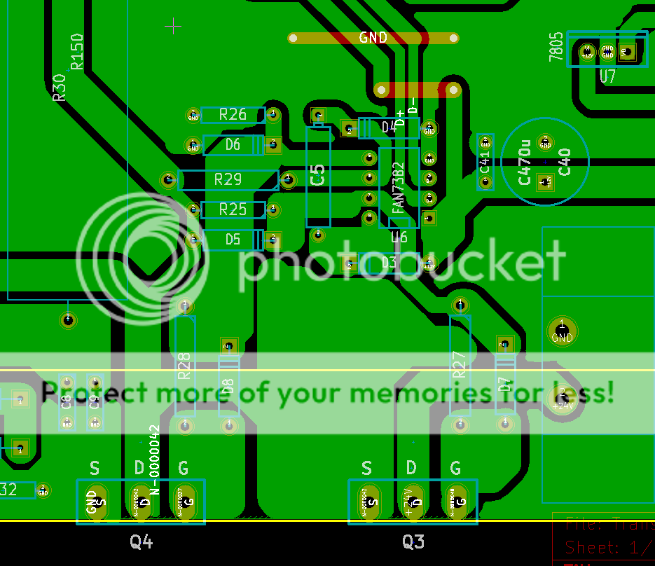
This is my layout of HVIC, D+ and D- are my differential PWM signal, generated by the 74 IC.

HVIC_Layout.png


Thanks for help !
 

I'm missing bus capacitors and a low inductance connection between U6 COM and Q4 source. Might cause parasitic switching and self oscillation at higher supply voltage levels.
 

Thanks for reply, I had connected the U6 com and Q4 source by soldering a wire, but it didn't help.

Is there anything I missed?

What if there is any problem in the +12V power for the HVIC and bootstrap cap to work?

- - - Updated - - -

You might need to buffer the gate drive to gt effective mosfet turn off, also what is the voltage rating of the diodes
D3, D4, ?

D3 and D4 I used are MUR160 (Ultra Fast Diode, D3 is used for charging Boot Cap and block the reverse voltage, and D4 is used for protecting HVIC from being harmed by Vs < -20V)

D5 and D6 I used are 1N4007.
 

It seems you may have overlooked the coupling factor from Vbulk (HV) to V bridge and Vboost
Add a series 10~100 resistor between FET out and Vbridge //Vboot_cap to limit current & ensure voltage does not exceed Absolute Maximum

VBRIDGE VHV: High Voltage BRIDGE pin −1 to 600 V
VBRIDGE −10 V Allowable Negative Bridge Pin Voltage for IN_LO Signal Propagation to DRV_LO (see characterization curves for detailed results)
VBOOT−VBRIDGE VHV: Floating supply voltage −0.3 to 20 V
 

Yes, add a 1uF cap with short leads from +HVDC to gnd right near the fets, also you have a lot of track on the main output, the higher dv/dt on this may be getting into your control and causing a VHF oscillation on the drive to the HB gate driver - causing the slower turn off on each fet, to reduce dv/dt on the output (at this time) try upping the 10 ohm turn on resistors to 47 to 100 ohm, if this lets you go higher than 130V then it is a dv/dt related problem, the output track is a real radiator of RFI.
 
It seems you may have overlooked the coupling factor from Vbulk (HV) to V bridge and Vboost
Add a series 10~100 resistor between FET out and Vbridge //Vboot_cap to limit current & ensure voltage does not exceed Absolute Maximum

VBRIDGE VHV: High Voltage BRIDGE pin −1 to 600 V
VBRIDGE −10 V Allowable Negative Bridge Pin Voltage for IN_LO Signal Propagation to DRV_LO (see characterization curves for detailed results)
VBOOT−VBRIDGE VHV: Floating supply voltage −0.3 to 20 V


Thank you for your reminding, sorry that I didn't update my schematic. In fact, I had it already.

I think your are mentioning the R29 resistor in my layout, which connect from the MOSFET output to the Vs in HVIC, for protecting the HVIC from being harmed by negative voltage.
 

D4 is somehow redundant (there's already the Q4 reverse polarised diode). Moreover, if D4 is faster than Q4 reverse diode, it would conduct (during the dead time) and might overload & destroy itself (depending on your output current).

I've seen some ringing on the gate signal. Maybe the dead time interval is too large and you only have the Q4 reverse diode (and D4) to manage the L1-C6 oscillations on the VS terminal of U6 during the dead time.

You have to shorten the dead time (avoiding the shoot-through anyway) to allow Q4 to create a low impedance circuit.

The gate ringing could also be reduced by a low impedance pulse capacitor (WIMA FKP 1 or something) across the HVDC bus.
 

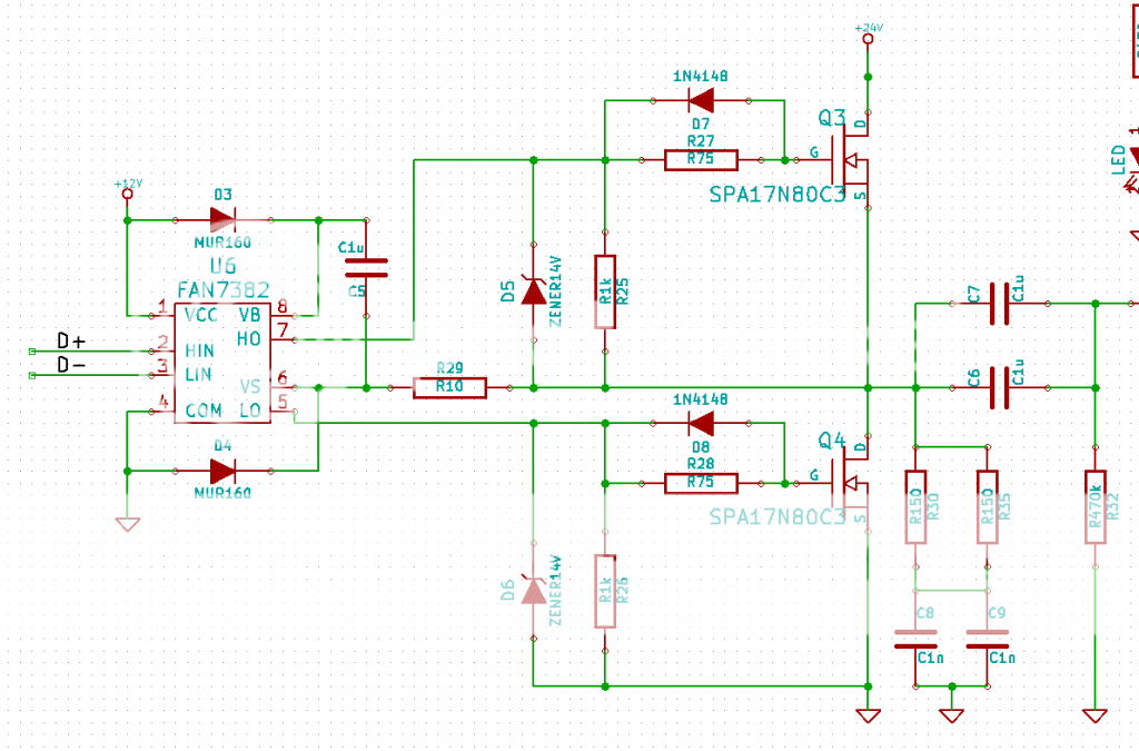
The circuit board shown does not appear to correlate to the schematic, R29 should be zero ohms,

Where are D5, R25 going to? Also D6, R26? a fix up of the hard ware needed.
 
The circuit board shown does not appear to correlate to the schematic, R29 should be zero ohms,

Where are D5, R25 going to? Also D6, R26? a fix up of the hard ware needed.

Thanks for reminding, I should update my schematic to avoid confusing.

HBridge-1.png


In my realization, I didn't attach D5 and D6, avoid the reverse charge on the D5 and D6 to build caps.
 

you have a lot of copper tracks connected to the output of the 1/2 bridge, this will radiate a lot of RFI on the switching edges and likely upset the control - this could be the root cause of your problems...

- - - Updated - - -

Isn't this on another thread also? You have a lot of copper track on the 1/2 bridge output, this makes a great antenna and will be radiating RFI at the switching edges and likely upsetting your control.
 
Anna, Thanks for your reply,

Finally I minimized the oscillation by adding a RC damping circuit between Gate and Source.

Do you have any suggestion in layout? Can it be optimized if I coat the Ground among the path of the Bridge OUT ?
 

Status
Not open for further replies.

Similar threads

Part and Inventory Search

Welcome to EDABoard.com

Sponsor

Back
Top