keremcant
Member level 5
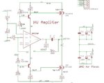
hi,
I have this circuit that amplifies the signal from a DAC to a piezoelectric. So I need high voltages at the output, more than 50V.
The HV in the schematic is 115V.
The op-amp used is op27, which takes max +-22V as supply and the voltages that I see are 15.2V, -12V.
the npn transistor is mje340, pnp is mje350
the problem is, I guess, that the when both IRF9630 and IRF630 are open, the node piezo+ cannot decide where to stabilize, 115V or -15V, since both transistors are open.
So what is the use of these mosfets? Also what is the use of the bjts?
A little explanation would be great.
thanks.