Continue to Site

Welcome to EDAboard.com

Welcome to our site! EDAboard.com is an international Electronics Discussion Forum focused on EDA software, circuits, schematics, books, theory, papers, asic, pld, 8051, DSP, Network, RF, Analog Design, PCB, Service Manuals... and a whole lot more! To participate you need to register. Registration is free. Click here to register now.

How to to drive P-Channel MOSFET at high side in 48V rail ?

Status
Not open for further replies.

giovaniluigi

Member level 1
Member level 1
Joined
May 30, 2009
Messages
32
Helped
0
Reputation
0
Reaction score
0
Trophy points
1,286
Visit site
Activity points
1,626
I need to drive a load with PWM using a P-Channel MOSFET and I need to supply current enough to drive the gate at high frequency whithout having too much loss.

The circuit is as follows:
highSideP.JPG

As faster as I can turn ON/OFF as less loss I'll have on the MOSFET.
The P Mosfet should be ON when the Vgs(th) > 2.5V but the Vgs(th) should not exceed 25V.
The problem is that the (VBAT) rail in the circuit above is 48V, when I pull the gate to GND it would destroy the MOSFET.
With the voltage divider and the zener diode I solve the problem, but the resistor also limits the current to the gate.

How can I drive the P MOSFET within the safe limits and also being able to provide let's say 200mA to the gate (if needed) ?
 

Use a buffer (e.g. complementary emitter follower) between Z-diode and gate.


Thanks for the tip.

There is something else that I should mention. The power rail ranges from 24V to 48V.
The resistor divider may be a problem because of that.

I found an appnote about that from TI.
There is something on it that I'm not understanding.
Please check the file: **broken link removed**

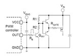
On page 20, they show a picture:
ti_PFET.JPG


After it, they say:

One of the drawbacks of this circuit is that V(DRV) is still a function of the input voltage due to the R1, R2 divider.
In most cases protection circuits might be needed to prevent excessive voltage across the gate-to-source terminals.
Another potential difficulty is the saturation of the npn level shift transistor, which can extend the turn-off time otherwise
defined by R1 and R(GATE). Fortunately both of these shortcomings can be addressed by moving R2 between the emitter of Q(INV)
and GND.
The resulting circuit provides constant gate driver amplitude and fast, symmetrical switching speed during turn-on and turn-off.

How moving the R2 to there will keep constant amplitude on gate ?
 
Last edited:

How moving the R2 to there will keep constant amplitude on gate ?
It turns the driver transistor into a constant current source, resulting in constant voltage drop across R1.
 

It turns the driver transistor into a constant current source, resulting in constant voltage drop across R1.

Sorry I don't get it.
When the transistor is off, the base current of the 'buffer transistors' will be set by R1.
When the transistor is on, the R2 will be 'added' to the circuit, forming a divider again which will set the base voltage and current of the buffer again.

What I'm missing ?
 

Sorry I don't get it.
When the transistor is off, the base current of the 'buffer transistors' will be set by R1.
When the transistor is on, the R2 will be 'added' to the circuit, forming a divider again which will set the base voltage and current of the buffer again.

What I'm missing ?
You are missing that the transistor is not fully on (saturated). With R2 in the emitter, the transistor acts similar to an emitter follower with the emitter voltage Ve a constant as determined by the input base voltage Vb (input resistor Rb is not needed). Thus the emitter current and consequently the collector current is determined by Ve across the emitter resistor R2 and doesn't vary significantly with the collector voltage (the collector acts as a high impedance current source). Thus the voltage drop across R1 due to this collector current also doesn't vary significantly with the supply voltage.

Note that you select the value of R2 to give the desired MOSFET Vgs ON voltage across R1 with whatever the high input signal level is (where Ic is (Vb-0.7V) / R1).
 
Correction to last post. The formula should be Ic = (Vb - 0.7) / R2.

Thanks for your explanation, now I'm understanding but there is something that is not right.
The Ic can be calculated as you mentioned, but the voltage to feed the buffer and mosfet will never be more than (Vb - 0.7).

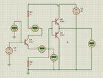
Please take a look on the following picture:
pFetDriver_Emitter.JPG

As you can see the Voltage at R2 is 2.6Volts.
Ic = 2.6 / 1000 = 0.0026 (ok)
Ve = ? R2 = 1k

To control properly the P-MOSFET I'll need to switch between 48V and (48-Vgs= 48-10) 38V.
 

but the voltage to feed the buffer and mosfet will never be more than (Vb - 0.7).
True, because you connected the buffer input incorrectly. It has to be connected to R1 instead, and R1 voltage drop has to be calculated for intended gate voltage, e.g. 10 or 12V.
 
True, because you connected the buffer input incorrectly. It has to be connected to R1 instead, and R1 voltage drop has to be calculated for intended gate voltage, e.g. 10 or 12V.

The problem is that the voltage drop on R1 changes with the rail.

24-48VOLTS.png

The idea is to not change with rail...
 

You're not measuring R1 voltage drop.

The voltage drop across R1 is Ic*R1, and essentially constant as long as the driver transistor isn't in saturation.
Constant voltage across R1 means constant gate-source voltage of PMOS, that's exactly what you want.

The measurement has to be made relative to rail voltage instead of ground.

Now I got it :) !

I'm so used to work with npn / n-channel that I forgot the P-channel.

Thanks.
 

Status
Not open for further replies.

Similar threads

Part and Inventory Search

Welcome to EDABoard.com

Sponsor

Back
Top