Continue to Site

Welcome to EDAboard.com

Welcome to our site! EDAboard.com is an international Electronics Discussion Forum focused on EDA software, circuits, schematics, books, theory, papers, asic, pld, 8051, DSP, Network, RF, Analog Design, PCB, Service Manuals... and a whole lot more! To participate you need to register. Registration is free. Click here to register now.

How to terminate a coplanar waveguide with 50 ohm load?

Status
Not open for further replies.

jameslast

Newbie
Joined
Feb 17, 2013
Messages
5
Helped
0
Reputation
0
Reaction score
0
Trophy points
1,281
Activity points
1,340
So I want to structure a coplanar waveguide by lithography, VNA - coaxial - picoprobe - coplanar waveguide transition to measure impedance of the waveguide. As signal and ground lines are on one surface, compared to e.g. a cpw without groundplane, one should be able to terminate the waveguide with 50 Ohm at the end on the wafer used for lithography?

I found some hinted ways to do this, e.g. different stub geometries, or an antenna or resistor as terminating load. The last one I know from BNC cables, the 50 Ohm ending caps. The correct stub geometry has probably to be found by something like CST Microwave, Sonnet, HFSS? My CPW consists of 100 nm thick gold, width 15 micron, gap 10 micron, 1-2 mm length, 1-2 GHz.

q7D6Bbj.png


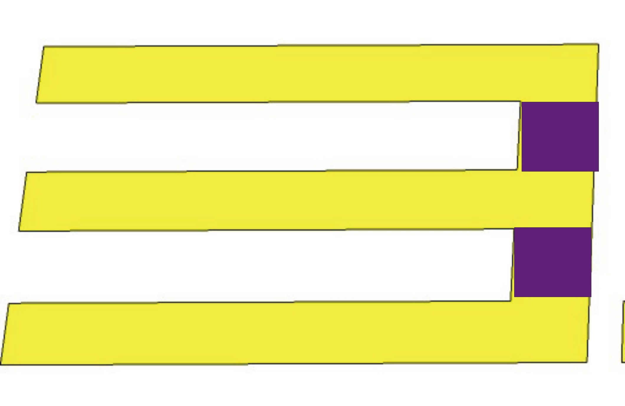
To find a material able to be deposited accurately with resitivity to yield 50 Ohm for this geometrical demands seems tricky like in the upper right of the picture. The lower left is my guess but probably wrong, causing reflections because of the 90° bended ground lines before ending in the stub, so maybe a tapering like in the lower right has to be designed or an antenna-like small coil?

Is there maybe a easier solution for this on-die termination, maybe to use unbalanced or coupled lines (sorry dont know exact name, basically CPW with 1 signal and 1 ground line). Maybe this is easier to design geometrically a terminating stub/antenna/resistor at the end?
 

Coplanar and other line types are special by having other than 50 Ohm characteristic impedance. The best option to measure their parameters with a standard 50-Ohm coaxial instrumentation is to use the transitions to coax or microstrp.
 

Yeah, there a better ways to measure impedance. Nonetheless for experimental reasons I have to choose picoprobes and terminate the coplanar waveguide on the Si-Wafer. And the 50 Ohm impedance of the line can be adjusted by setting width and gap of the cpw to appropriate values, but then the short circuit problem at the end of the cpw remains. So what is the best way to terminate the above cpw by approximately 50 Ohm? Thanks
 

Yeah, there a better ways to measure impedance. Nonetheless for experimental reasons I have to choose picoprobes and terminate the coplanar waveguide on the Si-Wafer. And the 50 Ohm impedance of the line can be adjusted by setting width and gap of the cpw to appropriate values, but then the short circuit problem at the end of the cpw remains. So what is the best way to terminate the above cpw by approximately 50 Ohm? Thanks

If you insist, I would make a lossy foil or block and set it around line end so that it will absorb all power without reflecting it. For similar cases I used a resistive metalized Mylar foil (50-300 Ohms/square) cut to a wedge and adjusted where desired while observing a swept response by a reflectometer. Any type of line can be terminated in this way. The only requirement is to use one-side 50-Ohm to a chosen line transition well matched over the desired frequency band.

Eccosorb and other absorber makers also offer lossy stickers to suppress unwanted reflections in MMIC enclosures. Cut a wedge and try, then press to hold in place. Do not care if such device has a specific impedance. It absorbs all power, this is what is needed.

Hmm, my understanding was it has to be 50 Ohm, otherwise I might get reflections and if I want to measure quantities like impedance change of this transmission line I get a lot of power losses due to the mismatch? What does "one-side 50 Ohm" mean exactly. Sorry physicist here, just diggin my head into microwave circuits. I'm able to deposit something like SiO2 or Si3N4 at the end of the coplanar waveguide or make the line 100nm or less which will increase the resistance to 50-200 Ohm to my knowledge (in this case probably only for a narrow band) So the SiO2 is probably better, this should absorb all power. My transmission lines only have a width of 10-20 micron, so I have to use lithography and physical vapor deposition to implement this termination. Also you say I shouldnt care about specific impedance but point to well matched 50 Ohm transition?

Sorry, really beginner here, unfortunately this submicron microwave circuits stuff is not really covered in books I found.
 

If it is a true coplanar line, i.e. NO ground plane underneath, the you need a balanced 50 ohm total load. None of your drawings would work well because of the extra inductance you are adding. You need two independent 100 ohm chip resistors.
 

What would be wrong with the upper right, when the brown part of the signal line actually represents a SiO2 piece, you mean instead of this I should terminate the the 2 ground lines with each 100 Ohm before short circuiting the signal line? And you are right, no ground plane, just gold lines on Si/SiO2 Wafer contacted by picoprobes.
 

if its an IC, then the one in the upper right corner may be fine. Because everything is so small...you probably do not have much inductance. But I was thinking something like this would have the highest frequency response:
 

yeah, thats what I was thinking of. I was googling to find some hints how this termination actually happens on very small IC in the nanometer regime where you have to do this by lithography & physical vapor deposition to position those terminations accurately and what kind of materials they use, I gues Si3N4 and SiO2. The experimental way would be to fabricate it by lithography, deposit and measure frequeny response with an VNA. But I was wondering what I can achieve here already by simulation or smart comments :) Do you know above software, are some of them able to simulate the frequency response of such a geometry, while I change for instance the termination material and geometry to get a broadband 50 Ohm termination? Because doing this with lithography in our lab would take some time
 

Status
Not open for further replies.

Part and Inventory Search

Welcome to EDABoard.com

Sponsor

Back
Top