Continue to Site

Welcome to EDAboard.com

Welcome to our site! EDAboard.com is an international Electronics Discussion Forum focused on EDA software, circuits, schematics, books, theory, papers, asic, pld, 8051, DSP, Network, RF, Analog Design, PCB, Service Manuals... and a whole lot more! To participate you need to register. Registration is free. Click here to register now.

How to properly terminate clock signal through a transformer

Status
Not open for further replies.

Hawaslsh

Full Member level 3
Joined
Mar 13, 2015
Messages
164
Helped
5
Reputation
10
Reaction score
7
Trophy points
1,298
Location
Washington DC, USA
Activity points
3,422
Hello all,

1659761824332.png

I am wondering what's the proper way to terminate a differential clock signal through a transformer into a single ended reference for a PLL. I've read through a few Ti application notes on the issue, but I am still a bit confused. The picture above is the diagram of what I am trying to accomplish. To generate a reference clock, there is a Ti clock distribution chip (LMK04208) creating a differential clock signal. The chip is capable of producing different types of clock outputs: LVDS, LVPECL, and LVCMOS. The PLL is an analog devices ADF4351, which has a single ended reference input. From the ADF4351 datasheet: "Reference Input. This CMOS input has a nominal threshold of AV DD /2 and a dc equivalent input resistance of 100 kΩ. This input can be driven from a TTL or CMOS crystal oscillator, or it can be ac-coupled"

There was a useful thread on the Ti design support forum about this topic, and one of the Ti folks recommended using a Mini-Circuits 1:1 transformer, TC1-1-13M+. However, the load in that case was 50 Ohms, not a high resistance CMOS input. In the case of the 50ohm load, the Ti rep said:
1659765112454.png

Does that imply I can simply terminate the single ended side with a 50ohm resistor placed close to the ADF4351 reference input? Is this value (or invalid) for all the different output types? If the 1:1 transformer can be terminated in 50 Ohms, does that imply I need to use 50 ohm differential impedance lines from the LMK04208 output to the transofmer as well as a 50 ohm line from the transformer to the ADF4351?

Any advice on the matter would be greatly appreciated,
Thanks in advance,
Sami
 

You'll either use a 100ohm:50ohm balun or 100 ohm termination at the unbalanced side, only suitable if cable between balun and Refin is short.

TC1-1-13M+ is a transmission line transformer balun, when connected as in your schematic it applies a common mode DC short to differential driver. Would need at least coupling capacitors. Better use a regular transformer, you definitely don't need multi GHz bandwidth in this application.

Refin must be AC coupled.

1659779672515.png
 

Hi,

Please mind the ADF4351 requirements:
datasheet says:
Input Sensitivity 0.7 AV DD V p-p Biased at AV DD /2; ac coupling ensures AV DD /2 bias

I´m not sure wheter your schematic of post#1 violates the max VPP specification,
but it surely violates the bias to AVDD/2 specification.

Klaus
 

Hello all,
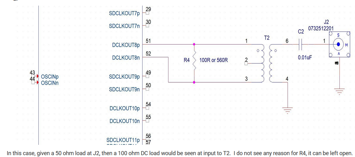
1659841674200.png

Thanks for the replies, very helpful. Quick follow up if you don't mind. If I am understanding your replies and the LMK04208 datasheet correctly. If I use the LVDS type output I can use the diagram above and achieve proper termination? The connection between the 100 ohm resistor and Refin would be very short, <5mm.
Input Sensitivity 0.7 AV DD V p-p
Hopefully I am understanding what the input sensitivity means. It means the reference signal must be greater than 0.7 Vp-p but less than AVdd Vp-p? I have an eval board of the LMK04208. I measured the LVDS output (single ended) with the scope set to 50 Ohm termination and measured 440mVp-p. This falls below the required input sensitivity , however, if I combine the differential output through a transformer I should get 2x 440mVp-p? Which would meet the sensitivity spec.

The LVCMOS type output measured 1600mVp-p (single ended with 50 ohm termination). This output type would give me a much larger margin to meet the sensitivity spec. However, the LMK04208 datasheet says nothing on how to terminate LVCMOS correctly. I found some other resources on how to terminate LVCMOS with simple 50 ohm transmission lines and 50 ohm resistors, however, all those resources were referring to single ended LVCMOS outputs. Would using the differential LVCMOS output be any different than my diagram above?


Better use a regular transformer, you definitely don't need multi GHz bandwidth in this application.
I only suggested the mini-circuits part because one of the Ti reps suggested one of their own products to convert a differential clock to single ended. Could you recommend a more economical part? As you suggested I dont need 3 GHz bandwidth. The max clock signal I would be generating is 125 MHz.

Thanks again for your help and time.
Sami
 

I measured the LVDS output (single ended) with the scope set to 50 Ohm termination and measured 440mVp-p.
Why are you using a 50Ω load?
The termination is determined by the transmission line impedance
What transmission line are you using, and how long is it?
 

Input signal with LVDS output level is only slightly above 0.7 Vpp requirement but may be sufficient.

100 ohm single ended line is hard to implement on PCB or as cable. Thus I suggested 2:1 balun.
 

Why are you using a 50Ω load?
Couple of reasons. My oscilloscope only has 50 or 1Mohm terminations. The eval board for the LMK04208 uses SMA end launch connectors. The eval board data sheet ( or user guide ) suggests so:
1659892913312.png

Sadly though, I'm no where near the 1 GHz BW or 10 Gsps rate :cry:
What transmission line are you using, and how long is it?
Sadly the user guide doesn't specify, nor does the schematic. I suppose I could use the gerber files and figure out the line impedance by measuring the trace widths/spacing and using the stackup on the gerber files... As for the trace lengths, they are pretty long, ~3 inches.

In all, i'll just use a 2:1 balun, 100 ohm diff lines and call it day. The user guide suggested a different balun than the Ti rep, sadly its 2x the price
 

that ref in port appears to be a dc coupled high impedance port. the data sheet shows needing a dc blocking cap of 1 nf there.

so you can not put your transformer to ground on that pin, you need to add a dc blocking cap.

on the side of the cap away from the pll chip, that is where you put the 50 ohm resistor. but you might not need one. In fact i would be tempted to send the clock to the board differentially, and put a 50 or 100 ohm resistor on the side of the transformer furthest from the pll chip. this may stop board ground plane noise from getting onto the ref in pin, as you no longer have a connection from the board ground plane to the ref in.

the transformer needs to pass digital signals, so make sure its bandwidth is at least 3 times the clock frequency, and preferrably higher.
 

the trace lengths, they are pretty long, ~3 inches.
That's not very long electrically.
The prop delay for a PCB trace is about 16cm/ns so 3 inches takes about 1/2 ns.
The general rule is that you only need termination resistors if the round trip propagation delay is equal to or greater than the signal rise/fall times.
So if the signal rise/fall time is greater than about 1ns, you should not need termination resistors.

You may be making things more complicated than needed.
 

That's not very long electrically.
3 inches (~72 mm) at 1 GHz??

That is very electrically long. At roughly 2 degrees per mm, you're looking at ~154 degrees. "Electrically long" is generally taken to be one-tenth of a wavelength, or 36 degrees.
 

3 inches (~72 mm) at 1 GHz??

That is very electrically long. At roughly 2 degrees per mm, you're looking at ~154 degrees. "Electrically long" is generally taken to be one-tenth of a wavelength, or 36 degrees.
it depends on your point of view. or more technically stated, on your SYSTEM DESIGN.

why do you care about 3" of length?
IF it is a digital signal at 50 gbps...yeah it matters.
if is is a digital signal at 10 mbps, not so much.

if it is an analog signal where you need an accurate phase shift at a wide range of rf frequenecies, it might matter.
If it is an RF signal with some complex modulation AND the device has a bad impedance (causing tripple transit interferrence) it might cause bit errors.
 

Status
Not open for further replies.

Part and Inventory Search

Welcome to EDABoard.com

Sponsor

Back
Top