Youncen
Member level 2
just be curious how to choose the w and l of a mos fet
http://photo.blog.163.com/photo/SzLFfkIsTscSLmAImidWgw==/1761188929278645092.jpg
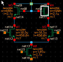
for example,in the pic,a larger l and smaller w campared to lower one is chosen to produce a lower common mode output voltage(hence a high output voltage swing),is it?
but
1.why not choose a pmos for the upper bias pair,it can offer more current gains
2.any idea about the middle one's channel modulation effect ? though a small length can offer the same Id at less cost of the area
3.if the technology is 350nano,is it always the preference to choose a small fet area nearly the minimum length or width of the technology regardless of any other design consideration, I mean bias mismatch etc
if other design considerations are respected,then what are they,how would the length or width chosen(for example how many multiples of the minimum length or width limitation)
thanks ~and again thanks [/img]
http://photo.blog.163.com/photo/SzLFfkIsTscSLmAImidWgw==/1761188929278645092.jpg
for example,in the pic,a larger l and smaller w campared to lower one is chosen to produce a lower common mode output voltage(hence a high output voltage swing),is it?
but
1.why not choose a pmos for the upper bias pair,it can offer more current gains
2.any idea about the middle one's channel modulation effect ? though a small length can offer the same Id at less cost of the area
3.if the technology is 350nano,is it always the preference to choose a small fet area nearly the minimum length or width of the technology regardless of any other design consideration, I mean bias mismatch etc
if other design considerations are respected,then what are they,how would the length or width chosen(for example how many multiples of the minimum length or width limitation)
thanks ~and again thanks [/img]