Continue to Site
Follow along with the video below to see how to install our site as a web app on your home screen.
Note: This feature may not be available in some browsers.
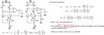
I wish to know how to get the formula, but I can't find it.
Does anyone know how to get this equation?
If you know how to derive the Formula (3) that in Paul Brokaw' paper, could you share it?