Continue to Site

Welcome to EDAboard.com

Welcome to our site! EDAboard.com is an international Electronics Discussion Forum focused on EDA software, circuits, schematics, books, theory, papers, asic, pld, 8051, DSP, Network, RF, Analog Design, PCB, Service Manuals... and a whole lot more! To participate you need to register. Registration is free. Click here to register now.

how to get the layout of a Silicon-Embedded transformer in momentum

Status
Not open for further replies.

mustangyhz

Member level 5
Joined
Nov 18, 2008
Messages
87
Helped
0
Reputation
0
Reaction score
0
Trophy points
1,286
Activity points
1,978
I know how to get the layout of a tranditional front-side on-chip transformer in momentum. But, I don't know how to get the layout of a Silicon-Embedded transformer in momentum, because the fabrication of the transformer is based on some special process including trench formation, thermal oxidation, trench filling, pad formation, backside metal removal and BCB layer formation.
transformer.JPG
help me!
thanks!
 

Attachments

  • ???2015A Silicon-Embedded Transformer for.zip
    1.2 MB · Views: 70

This requires "normal" Momentum stackup definition - except for the through silicon vias. These TSV need to be isolated from the conducting silicon substrate by some vertical oxide, and that is not possible with normal Momentum vias. But from what I have seen, Keysight have added some TSV functionality for Momentum in ADS2015. You should contact Keysight support and ask for more information on TSV simulation in Momentum.

~

Wait ... I see that vias and conductors are both embedded in silicon, with only a thin oxide layer as isolation. That is a lot of area and the capacitance is more critical then, compared to normal TSV cases. I don't know if the TSV approach in Momentum is accurate enough for this case. You should consider using the ADS 3D FEM solver instead of Momentum.

The oxide layers could be auto-generated from the Metal layers by using "derived layers". I had shown the use of these derived layers for auto-generating passivation here:
https://muehlhaus.com/support/ads-application-notes/ads-fem-3d-passivation
 
Last edited:
This requires "normal" Momentum stackup definition - except for the through silicon vias. These TSV need to be isolated from the conducting silicon substrate by some vertical oxide, and that is not possible with normal Momentum vias. But from what I have seen, Keysight have added some TSV functionality for Momentum in ADS2015. You should contact Keysight support and ask for more information on TSV simulation in Momentum.

~

Wait ... I see that vias and conductors are both embedded in silicon, with only a thin oxide layer as isolation. That is a lot of area and the capacitance is more critical then, compared to normal TSV cases. I don't know if the TSV approach in Momentum is accurate enough for this case. You should consider using the ADS 3D FEM solver instead of Momentum.

The oxide layers could be auto-generated from the Metal layers by using "derived layers". I had shown the use of these derived layers for auto-generating passivation here:
https://muehlhaus.com/support/ads-application-notes/ads-fem-3d-passivation

thanks for your reply!
can you give the substrate file in ads2011_10 for this work?
 

This requires "normal" Momentum stackup definition - except for the through silicon vias. These TSV need to be isolated from the conducting silicon substrate by some vertical oxide, and that is not possible with normal Momentum vias. But from what I have seen, Keysight have added some TSV functionality for Momentum in ADS2015. You should contact Keysight support and ask for more information on TSV simulation in Momentum.

~

Wait ... I see that vias and conductors are both embedded in silicon, with only a thin oxide layer as isolation. That is a lot of area and the capacitance is more critical then, compared to normal TSV cases. I don't know if the TSV approach in Momentum is accurate enough for this case. You should consider using the ADS 3D FEM solver instead of Momentum.

The oxide layers could be auto-generated from the Metal layers by using "derived layers". I had shown the use of these derived layers for auto-generating passivation here:
https://muehlhaus.com/support/ads-application-notes/ads-fem-3d-passivation


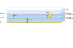
my substrate
substrate.JPG
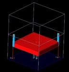
my transformer
3D-VIEW.JPG

Cu_mml resistivity of 3.9 μΩ-cm
conductivity
cu_mml.JPG
simulation results
S11.JPG

obiviously, it's wrong,
the resistance is too big! Do I set the wrong conductivity?
the primary coil is a capacitor! why?
 

This requires "normal" Momentum stackup definition - except for the through silicon vias. These TSV need to be isolated from the conducting silicon substrate by some vertical oxide, and that is not possible with normal Momentum vias. But from what I have seen, Keysight have added some TSV functionality for Momentum in ADS2015. You should contact Keysight support and ask for more information on TSV simulation in Momentum.

~


Wait ... I see that vias and conductors are both embedded in silicon, with only a thin oxide layer as isolation. That is a lot of area and the capacitance is more critical then, compared to normal TSV cases. I don't know if the TSV approach in Momentum is accurate enough for this case. You should consider using the ADS 3D FEM solver instead of Momentum.

The oxide layers could be auto-generated from the Metal layers by using "derived layers". I had shown the use of these derived layers for auto-generating passivation here:
https://muehlhaus.com/support/ads-application-notes/ads-fem-3d-passivation

Can you tell me what's wrong with my project in ads2011_10 momentum?
Thanks!
 

Attachments

  • mml_wrk.zip
    263.8 KB · Views: 68

I see, I set the wrong conductivity
Cu_mml
resistivity : 3.9 μΩ-cm = 0.039 μΩ-m


conductivity: 2.546e7 siemens/m
 

Status
Not open for further replies.

Part and Inventory Search

Welcome to EDABoard.com

Sponsor

Back
Top