kladenstein
Newbie level 5
Hello,
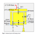
I have a frequency reconfigurable microstrip antenna project(2 to 6 GHz Multiband). There are two pin diodes in design(They change the length and provide reconfigurability according to their ON and OFF states). I drawed antenna in HFSS(i'm new to it) but as you know it's a passive device simulator. I need to export HFSS to ANSYS Insert Circuit Design (as the designer did in CST as the attached picture) for biasing circuit.
I actually can export it. But I don't know how to define ports(or terminals) for Pin Diodes in HFSS. I tried lumped port and wave port for that but they have no effect when analyze s11 of design in the Circuit Design.
- So, how do I need to define pin diode legs(terminals) in HFSS.
- and in HFSS do i need to add diode terminals(ports)on the antenna or tangent to the antenna slots as I did.
- or if everything I did is wrong can you tell me what I need to do?
(I hope I could explain my problem. Sorry for bad English.s )
The ones designer made.


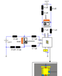
The ones I tried.

(second(top) diode has also the same structure I didn't show that)

(I drawed the biasing circuit arbitrary just to observe the effect. I'll change it to the right one).
Thanks.
I have a frequency reconfigurable microstrip antenna project(2 to 6 GHz Multiband). There are two pin diodes in design(They change the length and provide reconfigurability according to their ON and OFF states). I drawed antenna in HFSS(i'm new to it) but as you know it's a passive device simulator. I need to export HFSS to ANSYS Insert Circuit Design (as the designer did in CST as the attached picture) for biasing circuit.
I actually can export it. But I don't know how to define ports(or terminals) for Pin Diodes in HFSS. I tried lumped port and wave port for that but they have no effect when analyze s11 of design in the Circuit Design.
- So, how do I need to define pin diode legs(terminals) in HFSS.
- and in HFSS do i need to add diode terminals(ports)on the antenna or tangent to the antenna slots as I did.
- or if everything I did is wrong can you tell me what I need to do?
(I hope I could explain my problem. Sorry for bad English.s )
The ones designer made.


The ones I tried.
(second(top) diode has also the same structure I didn't show that)

(I drawed the biasing circuit arbitrary just to observe the effect. I'll change it to the right one).
Thanks.