Continue to Site

Welcome to EDAboard.com

Welcome to our site! EDAboard.com is an international Electronics Discussion Forum focused on EDA software, circuits, schematics, books, theory, papers, asic, pld, 8051, DSP, Network, RF, Analog Design, PCB, Service Manuals... and a whole lot more! To participate you need to register. Registration is free. Click here to register now.

How to draw footprint in MWO

Status
Not open for further replies.

kellyza

Member level 1
Joined
Jun 13, 2008
Messages
33
Helped
0
Reputation
0
Reaction score
0
Trophy points
1,286
Activity points
1,508
Hi all,

I would like to ask anyone out there on how to draw footprint of discrete component (both axial and chip type) using microwave office.

For your info, I'm designing a circuit consisting discrete elements such as transistor, resistor and capacitor. I'm not really sure how to draw the footprint using MWO. I have all the dimensions as in datasheet provided.

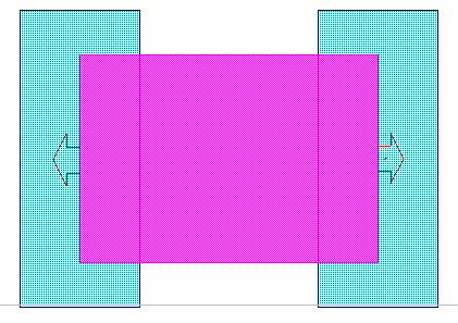
One more question, as in the layout, does it require some sort of stab or fan to connect the wire/txn line with the discrete component. I could not find that in MWO elements.

Thanks in advance.
 

Hello Kellyza,

Starting a New GDS Footprint Cell in MWO
Go to Layout Browser
Step 1: rigt click on Cell Libraries => select Create New GDS Library
Step 2: right click again on Your New Library to Create => New Layout Cell give any name
Step 3: Now Draw the footprint Layout & add the Cell Ports & save the cell

Now add your models such as FET or lumped element model in Schematic & change the layout properties to associate the correct footprint...
Note this customized footprint will be automatically highlighted based on the nuber of ports/nodes in the schematic & Cell ports in the Artwork editor...

See one of the MWO Getting started example in Chapter 5. MWO: Creating Layouts from Schematics Page # 11


---manju---
 
Thanks Manju...

Your explanation is very clear and helpful... I already created the footprint at the cell libraries and can use it in my circuit. My only concern is where exactly to put the cell ports and how to determine the suitable model layer such as nitride etch, air bridge, thick metal and whatsoever. I put the picture of one of the footprint I created for example (750 ohm resistor for case type 0805).

57_1289202472.png


Thanks again

---------- Post added at 08:55 ---------- Previous post was at 08:48 ----------

I don't have problems in creating the footprint for case/chip type component. However I really not sure or I could say that I don't know how to draw for axial type. May be anyone or Manju can help me solving the problem.

Thanks.
 

However I really not sure or I could say that I don't know how to draw for axial type. May be anyone or Manju can help me solving the problem.

Thanks.

It is nice to know that you are able to create artwork / footprints in MWO...
Regarding the other one...
upload your axial type artwork image so that we can help you to create in MWO...

---manju---
 

Ok... I just trying... I really do not know how to draw the axial type. This is the example that I've drawn.


This is for 442 Ohm axial resistor with the following dimension:
L max = 7.2 mm
D max = 2.5 mm
f min = 30 mm
d nom = 0.6 mm
PCB mounting centers = 10.2 mm
Min bend radius = 0.6 mm

Back to the cell port issue, did i put it correctly (for both case and axial type) or it is not suppose to be there? what about the material/model layer?

Thanks in advance.

---------- Post added at 02:21 ---------- Previous post was at 02:14 ----------

I also attach the physical data for you to clear. Mine is RC55 type.


Hello Kellyza,

for Case Type Cell Port help & validation see the examples available in the built in Artwork (foot print) library from "AWR Standard Chip Components.gds" by reading it as GDSII Cell Libraries...
C:\Program Files\AWR\AWR2010\Examples\Standard Chip Components.gds

Your Cell Port assignment for Case Type is correct but for Axial Type I need to check...
Let me see other replies...Then I will comment...

---manju---
 

Hi Manju...

Thanks for helping... can I ask you about 'via' and ground connection in MWO... usually via will connect from one layer to the other... if let say my design is just a simple microstrip which it involves 2 layers only then where to put the via? at all 'ground' in the circuit or at one of the 'ground' only? when a capacitor is connected to a ground then the capacitor in distributed circuit should be connected to where during simulation? Or just let it be opened? I'm not sure you understand or not with my question but pls ask if u need clarification.

I'm also waiting for others to give their comments...

There's always a light at the end of a tunnel...

-Kellyza-

---------- Post added at 08:59 ---------- Previous post was at 08:44 ----------

I hope the following figures make you clearer what am I asking.

=====>>>

=====>>>

Am I converted the circuit correctly from lumped to distributed circuit especially with the usage of VIA and MOPEN$ symbols.

Thanks.

-Kellyza-
 

Hello Kellyza,

You are absolutely correct !!!...see the below reference for conversion from Lumped to Distribute circuits in Microstrip...

Lumped / Distributed Transmission Line Element Conversions
RF Cafe - Lumped / Distributed Transmission Line Element Conversions
also this...
**broken link removed**

Yes, you need to use Via with groud for Inductor also you can model as loop meanderline for inductor equivalents in distributed justlinke in MMIC...
But verify the values from lumped to distributed network conversion for shunt Inductor XL=omega*L to Xl=Z0 *tan (theta)...

---manju---
 

OK... thanks Manju... I used txn line calculator to convert from lumped to distributed. What other design issues that I should put into account?

Just need some more clarification, what about the size of the via? Pls check this for me...

D ---> diameter of the via = width of txn line connected to the via
H, T and RHO ---> from the board properties

Pls correct me if I am wrong...

-Kellyza-

---------- Post added at 02:24 ---------- Previous post was at 02:13 ----------

for Case Type Cell Port help & validation see the examples available in the built in Artwork (foot print) library from "AWR Standard Chip Components.gds" by reading it as GDSII Cell Libraries... C:\Program Files\AWR\AWR2010\Examples\Standard Chip Components.gds [/QUOTE said:
I forgot to inform that I am using AWR2006 and I couldn't find the file you mentioned or may be it is in other folder... not so sure...
 

Hi Manju,

It seems everybody so quiet and not interested in giving their thought in this topic. By the way have you find ways on how to draw the artwork/footprint for the axial type?

Thanks
-Kellyza-
 

hi there,
im trying to design a wilkinson power dividert working at 1GHz ... i have a doubt , i hv added standard chip cells in the layout from GDSII library of 0805 size in the layout and im trying to extract an em structure. is ther any possibility to specify if the 0805 cell is a capacitor , inductor or a resistor and if so wer shud i give the capacitance or resistance or inductance values for the same..
 

Status
Not open for further replies.

Part and Inventory Search

Welcome to EDABoard.com

Sponsor

Back
Top