Continue to Site

Welcome to EDAboard.com

Welcome to our site! EDAboard.com is an international Electronics Discussion Forum focused on EDA software, circuits, schematics, books, theory, papers, asic, pld, 8051, DSP, Network, RF, Analog Design, PCB, Service Manuals... and a whole lot more! To participate you need to register. Registration is free. Click here to register now.

How to design a H BRIDEGE USING IGBT'S and its driver circuit for switching 230v dc

Status
Not open for further replies.

Logu KS

Member level 2
Joined
Jul 19, 2014
Messages
43
Helped
0
Reputation
0
Reaction score
0
Trophy points
6
Location
Chennai
Activity points
372
I need to switch 230v dc supply from the capacitor bank to load in clock wise and anti-clockwise direction (when the q1 and q3 igbts are ON the load should get +230v and when the q2 and q4 gbts are ON the load should get -230v from the capacitor bank).

The IGBT i am going to use is G160N60. I want to know which driver is suitable for performing the above mentioned operation. The H Bridge will be formed using the IGBT's.

As i am new to the power electronics i need guidance from the members of the forum.
 

Hi,

What did you do so far?

There are thousends of similar designs aroud...in this forum...and in the internet.
Even your IGBT manufacturer will provide informations in the datasheet and application notes.

You surely did read through them.
So, what's wrong with them?
Where do you see problem?

--> Please ask a specific question.

Klaus
 

Hi,

I have gone through many designs in this forum and found IR2110 is used as driver ic. But when i tried the half bridge circuit the Cboot gets charged when the low side switch is on but the charge gets discharged immediately. So, i couldnt get the output for the high side switching.

I tried many time and eventually the IR2110 IC gets heated. I tested with multimeter the LO out pin and vcc pins are shorted.

- - - Updated - - -

IR2110_halfbridge.png

this is circuit i initally tested..
 

Hello,that circuit works but the problem is that the output voltage is low,my self I tested and want to run full bridge SKM145GB066 and on the HO I get 6V and on LO I get very few about 600mV.

Dear Logu KS the High side(HO) is referenced on VS not ground
 

Hi,

but the charge gets discharged immediately.
The capacitor gets chraged. But the charge is limited.

Usually the gate of a FET /IGBT is very high ohmic. No DC current flow. But there is capacitance.
The bootstrap capacitance is much bigger than the FET capacitance, so it is easy to push enough charge to the FET´s gate without much voltage drop.

B U T:
With your circuit you have a 1kohms resistor connected. This resistor draws DC current and makes the bootstrap capacitor to empty within a short time.
The bootstrap capacitor shows a value of 100nF. so time constant is R x C = 1000 Ohms x 100nF = 100us.
Without the resistor it keepse the voltage easily 100 ...1000 times longer.

When you keep on datasheet you will see that the IR2110 does exactely what it should. Many many applications show this.
I also have good experience with the IR2110. Expectthe gate voltage at highe side (referenced to VS) max. 1V below VDD (referenced to GND).

Klaus
 

Hi Klaus,

Are you saying that if i remove that resistor the circuit will work fine.

I have one more doubt it is mentioned in all the threads and forums that the low side switched ON once in order to charge the bootstrap capacitor Cboot. But, in H bridge the transistor Q1 and Q4 are switched ON (for clockwise) at once and then Q2 and Q3 are switched ON (for anticlockwise). In such case, how Q1 will be switched on without Cboot having charge and same in next operation for Q3.

HO is referenced to VS and LO is referenced to ground.

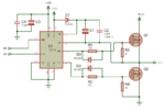
IR2110_Hbridge.png
 
Last edited:

Hi,

Are you saying that if i remove that resistor the circuit will work fine.
Try it.

In such case, how Q1 will be switched on without Cboot having charge and same in next operation for Q3.
Don't worry. Try it.
There are several scenarios...all will work.
The best solution is, that you i itialize your microcontroller port pins, enable the IR2110, and switch both IN signals to GND at the same time. This ensures that both bootstrap circuits get charged....Then start the PWM.

Driving HIN and LIN from seperate microcontroller pins is somehow dangerous.
The microcontroller pins usually are not configured during microcontroller start up. Maybe they are high impedance and catching up some noise. If both signals are recognized as high, then the Mosfets will be killed immediately. Within microseconds.

You could use the IR2110 enable pins to avoid this situation.
 

Hi,

Is it possible to perform the switching by giving voltage signal instead of PWM signal (By giving 12v to the HIN and LIN for switching)
 

Hi,

No.
Bootstrap supply can't work with DC.
You have limited time to switch ON the high side FET.
And you need at least a (very) short time where VS is 0V to charge the bootstrap capacitor.

Klaus
 

Can you explain me how to generate the control signals for HIN and LIN.
 

Hi,

LIN - HIN (description)
0 - 0 (at least a short time to avoid cross conducting)
1 - 0 (Low side ON. Also charges bootstrap capacitor)
0 - 0 (at least a short time to avoid cross conducting)
0 - 1 (High side ON)
Repeatedly

Klaus
 

I am asking whether the HIN and LIN signals can be given as 12v dc or not.

Giving 12v to LIN to switch on the Q2 which charges the Cboot by providing ground to Cboot.

Then giving 12v to HIN to switch the high side transistor. Same for the Q3 and q4.

If is is not possible can you explain me how to generate the signals for HIN and LIN. i.e., (0,0 0,1, 0,0 1,0) what you have mentioned in the previous comment.
 
Last edited:

I am asking whether the HIN and LIN signals can be given as 12v dc or not.

Giving 12v to LIN to switch on the Q2 which charges the Cboot by providing ground to Cboot.

Then giving 12v to HIN to switch the high side transistor. Same for the Q3 and q4.

If is is not possible can you explain me how to generate the signals for HIN and LIN. i.e., (0,0 0,1, 0,0 1,0) what you have mentioned in the previous comment.

HIN and LIN can get max 5V and are set by the microprocessor. Your circuit looks ok. Remember than HO is not measured from the ground- it is kind of floating. The width of the 0-1 and 1-0 pulses are determined by PWM. 0-0 pulses are of constant width.
 

Then my question is how to generate those pwm signals for controlling the switching. Using pwm ic's or using micro controller. I want to know how to generate those signals for controlling the switching operation.

My task is to provide the voltage from the cap bank to load by using two control buttons. While pressing one button the load is supplied with a +220 volt. While pressing another button the load should get the volt in opposite polarity (-220v). This signals can be manual as i said by pressing the button or it may be produced by the control device.
 

Hi,

Using pwm ic's or using micro controller
The short answer is given in the post before:
HIN and LIN can get max 5V and are set by the microprocessor.

The long answer is:
We don´t know what microcontroler you use. So we don´t know if it is able to generate PWM signals.


***
PWM...
Is a digital signal. High and Low.
It is defined with:
* Low voltage level
* High voltage level
* PWM frequency
* duty cycle

It´s on you to define it.

Klaus
 

I am going to use PIC16F877A microcontroller. But, i dont know how to generate pwm signals using microcontroller.

Kindly provide me the guidelines for generating the pwm signal using the PIC microcontroller for the switching operation.
 

Hi,

I never used PIC.
* But I remember a lot of discussions here in this forum.
* Microchip will have informations in their datasheets, and they will have application notes.
* There are a lot of example designs in the internet.

Klaus
 

I am going to use PIC16F877A microcontroller. But, i dont know how to generate pwm signals using microcontroller.

The microcontroller has two PWM pins with 10 bit resolution. PICs are very easy to program but YOU must read the manuals because there several small details that are scattered all over the manual. This is a 44 pin pack and you must have some provision to update the software once the board has been made. Once you decide to use PWM it will tie up one timer because the pulse width will be taken from the timer registrar. These details can be worked out but you need to set up a clear flowchart for this part at least...
 

In addition, although being a bit obvious, it is quite advisable to create timer interrupt at each completion of the PWM period cycle. This way, you’re able to monitor the output, sample-by-sample, making on time proper mathematical adjustments on duty-cycle according to the actual value just read.
 

First you need to figure out the operation frequency at the driver input.

Next you need to select the osc frequency for the microcontroller.

Set up the PWM channels.

Set up the ADC channel (just in case you want to monitor the current). Even if you are not using it right now, just keep a hook.

Set up the array for the PWM widths that will be running in a loop.

Include in the array suitable dead intervals when both the outputs are off.

Check on the scope that you are getting the pulses as expected.

Connect the output of the PWM to the driver module.
 

Status
Not open for further replies.

Similar threads

Part and Inventory Search

Welcome to EDABoard.com

Sponsor

Back
Top