Continue to Site

Welcome to EDAboard.com

Welcome to our site! EDAboard.com is an international Electronics Discussion Forum focused on EDA software, circuits, schematics, books, theory, papers, asic, pld, 8051, DSP, Network, RF, Analog Design, PCB, Service Manuals... and a whole lot more! To participate you need to register. Registration is free. Click here to register now.

[SOLVED] How to choose the value of current mirror bypass capacitance?

Status
Not open for further replies.

fuxinmingming

Member level 1
Joined
Nov 2, 2007
Messages
36
Helped
0
Reputation
0
Reaction score
0
Trophy points
1,286
Location
China
Activity points
1,538
Hi guys,

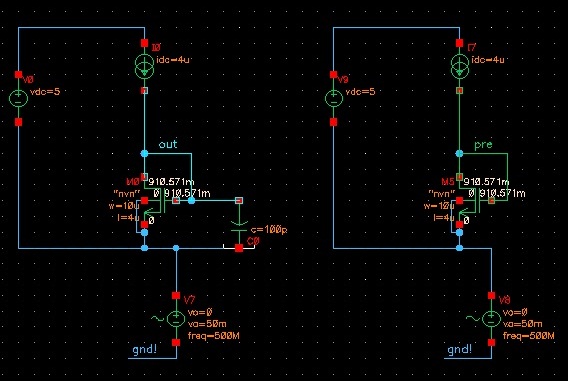
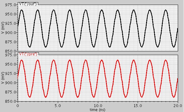
When we use current mirror, usually we add bypass capacitance to reduce bias branch's noise.

For example, if I add 500fF bypass capacitance, total noise will be reduced by almost 10 times(noise=kT/C, capacitance increased almost by 10 times).

My question is:
How should I choose this bypass capacitance? Is it semiempirical? Is it 500fF capacitance ok? Or how do I calculate its value?

Regards,

Ming
 

I don't think thermal noise is the only nor the main concern, I would rather think of crosstalk and supply noise. This is what bypass usually helps with. Also lowering the impedance of the bias voltage generator is an option to consider. Sizing will depend on your major contributors.
 

Hi dgnani,

firstly, thank you for your reply.

I would rather think of crosstalk and supply noise

What do you mean by crosstalk and supply noise? Could you explain it in detail?

Regards,

Ming
 

Hi guys,

In order to make it clear, I put the circuit here. I add a sine wave(50mv, 500MHz) to the ground and compared the original circuit(no bypass capacitance) and the circuit adding bypass capacitance. Through simulation, there is no different between the voltage bias. It confused me. Pls help. Thanks.


Regards,

Ming

---------- Post added at 13:37 ---------- Previous post was at 13:32 ----------

Hi guys,

This is the ac analysis results from ground to node pre and node out. Please check it.


Regards,

Ming
 

Hi Ming,

I will try to have a look later for now please notice that your AC analysis did not work, you are only getting numerical noise: you need to have an AC source (not a regular sinusoidal source), you should be able to set that directly inside your sinusoidal source; if that is a vsin source from analogLib (that is you are working in Cadence) you should have an 'AC Amplitude' field in your source...
 

Hi dgnani,

I simulated the circuit in Candence. And for the AC analysis I set sinusoidal source's AC Amplitude to 1V.

Regards,

Ming
 

Hi Ming,

my bad, your result is as expected, basically a flat 0dB (+numerical noise): all noise on gnd appears on the bias line at any frequency, in this case the capacitor is of no help whatsoever. Still if the cap was decoupling to a different, quiet supply line (AC ground) then the larger the cap the smaller the noise on the bias line at high frequency. The high frequency value of vb/vss would be Cg/(C+Cg), where Cg is (mostly) the gates' capacitance on the bias line, and C is the decouling cap. The pole of vb/vss is gm/(C+Cg), which shows how increasing gm can help filtering lower frequency noise once C cannot be increased any further.
The same would happen if the gate receiving the bias is far from the driving diode-connected device: noise on the bias generator ground could be filtered by a cap close to the biased device.
Similarly you can see that adding capacitance to the bias line helps with crosstalk noise coming from neighboring nets (e.g. model it with an AC source and cross-coupling cap)
 
acctually, this cap together with the 1/gm of diode connected mos device forms a low freqency pole for voltage mode. For current point of view, this cap is acctually a 1/wc shunt current path.
 
Hi dgnani and tdy,

Thank you for both of you. It helps me a lot.

Regards,

Ming
 

Status
Not open for further replies.

Part and Inventory Search

Welcome to EDABoard.com

Sponsor

Back
Top