Continue to Site

Welcome to EDAboard.com

Welcome to our site! EDAboard.com is an international Electronics Discussion Forum focused on EDA software, circuits, schematics, books, theory, papers, asic, pld, 8051, DSP, Network, RF, Analog Design, PCB, Service Manuals... and a whole lot more! To participate you need to register. Registration is free. Click here to register now.

How to calculate the propagation delay of a circuit?

GreatField

Newbie level 6
Newbie level 6
Joined
Mar 13, 2022
Messages
14
Helped
0
Reputation
0
Reaction score
0
Trophy points
1
Activity points
120
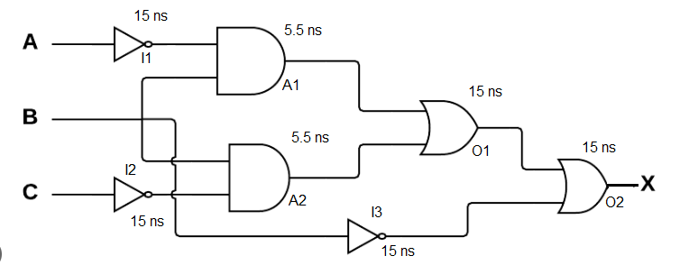
Suppose the circuit below, where each logic gate has a propagation delay given by (tPLH + tPHL) / 2.

propagation-delay.png


The correct method of calculating the circuit's propagation delay would be to add the gates that take the longest time to reach the output, which in this case would be:
I1 + A1 + O1 + O2 = 50.5 ns ?
 
Hi,

basically correct.
You need to calculate each path:
A->X
B->X
C->X

but ... the circuit includes some issues.
The minor issue is: Why does the signal B cross two other signals. If yu re-order the signals (A-C-B) you omit the 2 crosspoints and the circuit gets much simpler to read.

Then the major issue becomes visible:
The bottom input of A1 as well as the top input of A2 is not driven. With this the input level is not determined .. and thus the output is not determined.
So the whole output X is not determined. So the whole circuit makes no sense.

Now one may guess that there is a junction point missing, that connects B with the inputs of A1 and A2. But I don´t think so, because then the signal B on it´s way to I3 crosses itself. No one would draw it this way.

Klaus

I took this circuit as an example from Google just to check if the calculation method was correct. Thank you for clarifying my doubt and pointing out the problems in the circuit


Thanks
 
TPLH and TPHL are often unequal and also vary gate-to-gate
and gate-w/-load by construction. The result of any such
figuring will not match any particular path through the
schematic.

The next step up the ladder would be to assign for each output
node, from the input conditions, the expected transition and
its direction-delay. If you knew them separately. You might find
the exercise interesting. Or not, depending on goals.
 

LaTeX Commands Quick-Menu:

Similar threads

Part and Inventory Search

Welcome to EDABoard.com

Sponsor

Back
Top