Welcome to our site! EDAboard.com is an international Electronics Discussion Forum focused on EDA software, circuits, schematics, books, theory, papers, asic, pld, 8051, DSP, Network, RF, Analog Design, PCB, Service Manuals... and a whole lot more! To participate you need to register. Registration is free. Click here to register now.
here cox = Eo/Thickness of oxide layer
and then cgso is actually the capacitance at no channel so you wud have to add this cgs with cgso in order to find it correct.now this cgso is provided in transistors specifications,and moreover since we short the bulk to source therefore we often neglect that capacitance
actually if you wanna find the total CGS thats the gate to source capacitance then first there will be a capacitance from gate to drain(or source) secondly due the the overlap of drain/source just beneath the oxide layer has a certain capacitance thats pretty obviously dependent on the Xd i.e thickness (the overlap) so it would be cgso=Cox*W*Xd now you can get the total source capacitance by adding cgs(i.e capacitance between gate an source other then the overlapping part)+cgso(i.e overlaping one)=CGS
with no channel i meant that its not the one thats dependent on channel its basically the overlap one,when the channel is formed then the current flows and after that the parasitic capacitance (of drain or source could be felt at some conditions).
thirdly,there is a capacitance thats called junction capacitance ,between drain and bulk because the depletion region between drain and bulk serves as a dielectric medium between those two material,but assume that the drain and bulk are at same potential then why would there be any capacitance when theres no opposite polarity of plates?? how could a dipole be formed in a simple capacitor when both plates are at the same charge?? ,so thats what happens when we actually short bulk and source.
bro i cannot find where CGS=CGSO but if its there then it could be because of no potential applied or the potential at drain/source would be so low that its parasitic capacitance might have been neglected for simplicity.
hope it could help
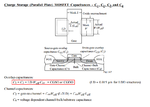
This is where i find CGS=CGSO . After i read your post, i found that this pic just wants to illustrate overlap cap. and i misread it to Cgs = Cgso.
and i think this pic is wrong , it should be CGS=CGSO*Weff.
Mask W and Actual W, which one is the width of nmos we usually talk about?
and this pic is the answer:
after my calculation, i found that the overlap one is about 1/1000 of non-overlap part. So i think it could be ignored in most cases.
np np bro
no the CGS will not be CGSO*Weff,the CGSO is itself a complete capacitance,what is done is Cox*Weff*L(here Cox=(Eo/thickness)=(C/A)) now if you multiply the capacitance with a dimension then it wont be the capacitance on a surface of some area it would be something else.
This site uses cookies to help personalise content, tailor your experience and to keep you logged in if you register.
By continuing to use this site, you are consenting to our use of cookies.

")