newbie_hs
Full Member level 1
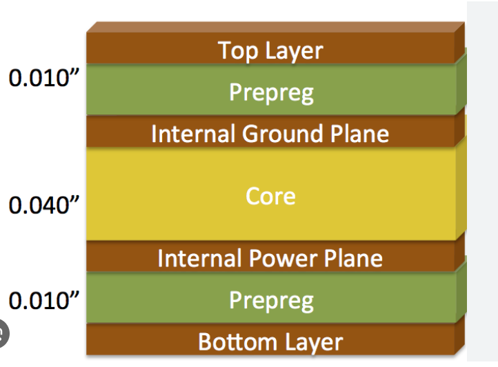
In some pcb stackup's I can see that the power plane is given as reference to signal layers.
I have some questions regarding this.
1) May I know in that case how the return current flows.
2) Assume all my signals present in the layer belongs to 1.8V and I am proving a 3.3V power plane as reference. Will it cause any SI issues.
Below is an example of a stackup where power plane is given as reference to bottom signal layer.This is just for a refrence