Continue to Site

Welcome to EDAboard.com

Welcome to our site! EDAboard.com is an international Electronics Discussion Forum focused on EDA software, circuits, schematics, books, theory, papers, asic, pld, 8051, DSP, Network, RF, Analog Design, PCB, Service Manuals... and a whole lot more! To participate you need to register. Registration is free. Click here to register now.

how much diode area should be choosed for ESD protection

Status
Not open for further replies.

xianweng

Member level 1
Member level 1
Joined
Aug 26, 2011
Messages
33
Helped
0
Reputation
0
Reaction score
0
Trophy points
1,286
Visit site
Activity points
1,535
hi,everyone
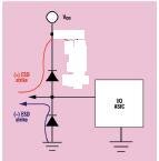
how to choose diode area for ESD protection?For example ,if i want to pass HBM 2kV and the transient maximum 1.33A,how much area could withstand such a big current? Are there other factor should be considered when choose diode area?For example diode technology as below
Thanks any help in advance
esd_170.jpgQQ截图20141110111402.jpg
 

First, this is not about one diode. It is about the current
loop and every device it must traverse to get from its
entry to its exit. "Victim" devices exist all around the loop
and have different voltages imposed by the local drops /
rises. You really want reliable, reasonable models for the
protection and the "victim" devices which include breakdown
behaviors. You are likely to be disappointed, there, and may
have to pull your own TLP data and fit your own model
unless your foundry is unusually elnightened and supportive
of explicit ESD protection design (rather than, say, giving
you three cells and a page of generic advice and no more).

If you have good device models and a good circuit for the
loop (and there is certainly more than one unless your
chip design is trivial) then you can explore the area effect
on imposed voltage in simulation. This has to be verified,
not assumed.

If you figure that 2kV HBM is about 1.5A, then you may
be able to figure or simulate the diode forward drop at
that current. The more critical and interesting bit is the
central clamp (which it looks like you have whited-out)
which determined the amplitude of the positive strike's
voltage applied to the positive supply rail (or ESD+ ring,
depending on whether you are using the VDD as one leg
of the protection ring, or making that independent).
This voltage threatens the entire chip core and will seek
out the weakest link chip-wide. Here you depend critcally
on breakdown attributes and, if it's an active clamp, its
turnon speed and on-resistance. Do not ignore the effects
of the trailing edge, an active clamp that turns off too
soon can release against a still-significantly-charged
HBM source and still allow damage. In low voltage
technologies the clamp breakdown "backstop" voltage
may be to high to protect gate oxides and the dynamic
action is all there is. It needs to persist until the source
voltage has been discharged below gate ox breakdown
(which for low voltage technologies is many, many
tau_HBM).
 
Status
Not open for further replies.

Part and Inventory Search

Welcome to EDABoard.com

Sponsor

Back
Top