Continue to Site

Welcome to EDAboard.com

Welcome to our site! EDAboard.com is an international Electronics Discussion Forum focused on EDA software, circuits, schematics, books, theory, papers, asic, pld, 8051, DSP, Network, RF, Analog Design, PCB, Service Manuals... and a whole lot more! To participate you need to register. Registration is free. Click here to register now.

How does this UART to RS-232 converter work?

Status
Not open for further replies.
The AVR circuit in post #1 is apparently inverting RxD in software, it uses pin 18 instead of dedicated UART pin 14. At least AM7910 would need an external inversion, the modem chip has no option to provide it.
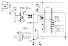
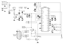
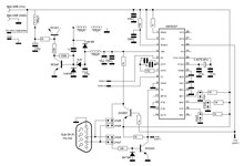
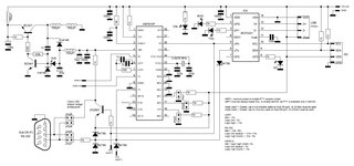
FvM, you mean it inverts in software the data sent from pin 18 of the microcontroller (post#1), which then drives the RxD pin in the D-sub9 connector, right?
So it is the signal in the base of T2 that has to be inverted in that microcontroller schematic.
 
Last edited:

Hi,

The signal flow is:
from D-SUB --> R1 --> Microcontroller_pin15 (SW-RxD)

There is no hardware inverter. Thus the inversion needs to be done in SW.

Microcontroller_pin15 is not the dedicated UART_RxD. Thus one can assume that the UART is implemented in software.
(Not the internal HW periferal). Thus the polarity is not the typical UART polarity.
For the SW-UART the inversion is no big deal.

Klaus
 

    neazoi

    Points: 2
    Helpful Answer Positive Rating
Hi,

The signal flow is:
from D-SUB --> R1 --> Microcontroller_pin15 (SW-RxD)

There is no hardware inverter. Thus the inversion needs to be done in SW.

Microcontroller_pin15 is not the dedicated UART_RxD. Thus one can assume that the UART is implemented in software.
(Not the internal HW periferal). Thus the polarity is not the typical UART polarity.
For the SW-UART the inversion is no big deal.

Klaus
Ok, so in the modem circuit, I think, after your suggestions, I got it right this time.
Please note the TTL/modem/RS-232 signal levels chart at the right of the picture, I think I got this right now.

Let me know if you see any problem on these.

Thank you
 

Attachments

  • modem3.JPG
    modem3.JPG
    168.7 KB · Views: 108

Hi,

I see some issues:
* I think you mixed Tx and Rx. See my signal flow from post#22. The signal goes to RxD, but yours go to TxD
* The BJT 2N2907 needs a base resistor
* SCL as well as SDA need pull up resistors.

While you can route the incoming signal to many RxDs (inputs to microcontroller, USB_UART) .. you can´t do the same with several TxD =output signals. Combining multiple outputs create short circuit currents. Better use AND gate to combine them.

Didn´t go deeper..

Klaus

Sorry about the lengthy post, I am just trying to cover your points.

>>>* I think you mixed Tx and Rx. See my signal flow from post#22. The signal goes to RxD, but yours go to TxD

This one relates to your last paragraph. The modem chip is the "master" let's say. It is from this and to this that all other ports should send/receive data. I am not using this circuit as a conversion from one port/protocol to the other.

Pin 26 in the modem is an output, which is connected to RX in UART and Urx in the USB chip. It is connected to the input of the inverter and then to the TX pin of the RS-232 port.

Pin 10 in the modem chip is an input, which is connected to the TX of the UART and the Utx of the USB chip. It is also connected to the RX pin of the RS-232 port, after the limiter.

Do you see any problems on these?


>>>* The BJT 2N2907 needs a base resistor

Thank you. I have added the resistor and re-attached the schematic.


>>>* SCL as well as SDA need pull up resistors

I thought I will leave these to the external sensors/devices, but yes you are right. I have added these in the attached schematic.


>>>While you can route the incoming signal to many RxDs (inputs to microcontroller, USB_UART) .. you can´t do the same with several TxD =output signals. Combining multiple outputs create short circuit currents. Better use AND gate to combine them.

That's a tricky one. Indeed data out of the modem is routed to all the ports SIMULTANEOUSLY.
But on TX, I thought I will have the user to manually transmit in just one of the ports, not all ports simultaneously. Now transmitting in one port, may in fact interrupt other TX ports like you mention. For this reason, I added two low voltage drop diodes, one at the TX pin of the USB chip and one at the TX pin of the UART pad.
This would isolate these two ports without introducing too much voltage drop to affect logic 1?

However, I did not do the same for the RS232 port, because of the marginal voltage levels there. A negative voltage at the limiter diodes coming from the RS232 port, will be routed to the ground by the reverse diode and hopefully won't affect other ports.
A positive voltage at the limiter diodes coming from the RS232 port, won't reach the USB and uart port.
However, a positive vvoltage from the USB and UART ports will be fed back to the RS-232 TX pin. Whether or not this will create problems (currents like you described) I do not know.
When I tested some other rs232 devices by shorting both TX and RX ports pairs, nothing bad happened, it just did not work, and this was expected of course.
 

Attachments

  • modem4.JPG
    modem4.JPG
    174.1 KB · Views: 104

Hi,

OK. Maybe a misunderstanding from my side....

So Modem_RD is an output. It should go to
* RS232_output (according my understanding this is UART_Tx, but you named it Rx)
* and USB_UART_URx (which is an input)
.. so far the wiring is correct

Modem_TD is an input. it should get it´s data from
* RS232_input (according my understanding this is UART_Rx, but you named it Tx)
* and USB_UART_UTx (which is an output)

Here I see a problem. Two "sender" should go to one receiver.
I said you should use an AND to combine both signals.
I see you used a diode (next to USB_UART_UTx).
The way it is oriented it rather generates a WIRED_OR than an AND.
--> You have to rotate it.
--> you need to add a diode from RS232_input to the MODEM_TD node
--> and you need to add a Pull_up at the MODEM_TD node to prevent the signal from floating.
Mind: UART signals are idle HIGH.

I don´t know what´s the use of the BAT85 next to the text "TXD (UART)"

Klaus
 

The purpose of the RS232 connector is unclear. Presently the jumpers aren't fitted, so no problem. The modem can work with USB-to-UART bridge.
 

Hi,

OK. Maybe a misunderstanding from my side....

So Modem_RD is an output. It should go to
* RS232_output (according my understanding this is UART_Tx, but you named it Rx)
* and USB_UART_URx (which is an input)
.. so far the wiring is correct

Modem_TD is an input. it should get it´s data from
* RS232_input (according my understanding this is UART_Rx, but you named it Tx)
* and USB_UART_UTx (which is an output)

Here I see a problem. Two "sender" should go to one receiver.
I said you should use an AND to combine both signals.
I see you used a diode (next to USB_UART_UTx).
The way it is oriented it rather generates a WIRED_OR than an AND.
--> You have to rotate it.
--> you need to add a diode from RS232_input to the MODEM_TD node
--> and you need to add a Pull_up at the MODEM_TD node to prevent the signal from floating.
Mind: UART signals are idle HIGH.

I don´t know what´s the use of the BAT85 next to the text "TXD (UART)"

Klaus

Regarding the opposite markings of the UART pins you are thinking that the Utx of the USB chip goes to the RX of the UART. This is true when you connect JUST these two ports together.
But in this modem, one side is the modem IC and the other side are all the rest of the ports/standards. These ports all listen to the same data that comes out of the modem IC. Each of these ports can transmit data ONLY to the modem, not in between them. So the TX pin of one port cannot be connected to the RX pin of the other. Transmitting data between the ports (if one wants to use the circuit to convert TTL to USB for example) will be done only through loopback audio of the modem, so as to avoid having many switches for lots of configuration. Data is only half duplex.

The thing about the gate, I have seen the gate you propose, but I am not sure how it will be connected in the different parts of the circuit. Perhaps it is better for you, to save writing and time to quickly edit the drawing of the schematic to explain the connections? If this is of not trouble to you I would love to.
--- Updated ---

The purpose of the RS232 connector is unclear. Presently the jumpers aren't fitted, so no problem. The modem can work with USB-to-UART bridge.
But then you need another chip, don't you?
 

Hi,

Regarding the opposite markings of the UART pins you are thinking that the Utx of the USB chip goes to the RX of the UART.
this "you are thinking" sounds like "guessing". But I just follow your schematic.
USB_UART_UTx is connected (somehow) to th RS232_Rx.
* without the diodes the USB_UART overrides all informations coming from RS232. --> The RS232_Rx never can send data to the modem.
* with the diode installed (the way you did in your schematic), forces the modem_Td node to be HIGH. No change for the RS232_RX to work. Only if the USB_UART_UTx is LOW (which usually not is) the RS232_Rx can work.

AND gate: 2 inputs, 1 output
* Each sender sends it´s signal to the AND_inputs individually.
* the AND_output sends it´s signal to the receiver (what I guess the modem_TD is).


Klaus
 

    neazoi

    Points: 2
    Helpful Answer Positive Rating
Hi,


this "you are thinking" sounds like "guessing". But I just follow your schematic.
USB_UART_UTx is connected (somehow) to th RS232_Rx.
* without the diodes the USB_UART overrides all informations coming from RS232. --> The RS232_Rx never can send data to the modem.
* with the diode installed (the way you did in your schematic), forces the modem_Td node to be HIGH. No change for the RS232_RX to work. Only if the USB_UART_UTx is LOW (which usually not is) the RS232_Rx can work.

AND gate: 2 inputs, 1 output
* Each sender sends it´s signal to the AND_inputs individually.
* the AND_output sends it´s signal to the receiver (what I guess the modem_TD is).


Klaus
All right I see what you mean now. Because the idle state is 5v...
All right I will try to do this gate and come back to you with another schematic.
"You are thinking" I did not mean to be rude, it's not my native language :)
 

Hi,
"You are thinking" I did not mean to be rude,
Thanks for this response. Please do the same if you are not sure next time.

No, no. I didn´t see it as rude either. (not my native language, too)
I just wanted to clarify that it was not just a weak feeling that it may cause problems, instead I´m pretty sure it does not work the way you expect it.

(Hopefully) I´m more focussed on solving technical problems. Help those who show that they are busy doing their project.

All is well.

Klaus
 

But then you need another chip, don't you?
As many contributors stated since the thread start, the input from RS-232 jack has to be inverted.

Also, if you have multiple sources driving modem TD input, they need to be switched by a mux or at least AND logic, as suggested by KlausST. In the latter case, you need to assure that not more than one source is driving "space" state (low level) at the same time.
 

    neazoi

    Points: 2
    Helpful Answer Positive Rating
As many contributors stated since the thread start, the input from RS-232 jack has to be inverted.
I see what you mean, the receive pin.
How about this schematic? (ignoring the other chip for a while)
Will it do?
 

Attachments

  • modem5.JPG
    modem5.JPG
    112.2 KB · Views: 91

It should work fine. The clamp diode to +5V can be omitted, because the transistor BE-diode is already limiting the voltage to 0.7 V. I would also increase input series resistor to 10k.
 

It should work fine. The clamp diode to +5V can be omitted, because the transistor BE-diode is already limiting the voltage to 0.7 V. I would also increase input series resistor to 10k.
If I omit this clamp diode, 5v will pass directly to the NPN base.
And the NPN will be permanently ON.
Are you sure?
--- Updated ---

If I omit this clamp diode, 5v will pass directly to the NPN base.
And the NPN will be permanently ON.
Are you sure?
UPDATE:
I have totally removed the two clamp diodes. The NPN will not conduct on negative voltage on the base, so there is no meaning for these diodes there.
Does it seem ok now?
 

Attachments

  • modem5.JPG
    modem5.JPG
    109.7 KB · Views: 87
Last edited:

You should better follow my previous suggestions. -12V RS-232 level exceeds BE negative voltage rating and at least degrades transistor current gain or even damages the transistor.
 

    neazoi

    Points: 2
    Helpful Answer Positive Rating
You should better follow my previous suggestions. -12V RS-232 level exceeds BE negative voltage rating and at least degrades transistor current gain or even damages the transistor.
Thanks, I havent's thought that. Ok I re-inserted the negative clamp diode and changed the NPN base resistor to 10k.
It should be ok now I guess.
 

Attachments

  • modem5.JPG
    modem5.JPG
    108.3 KB · Views: 83

Status
Not open for further replies.

Similar threads

Part and Inventory Search

Welcome to EDABoard.com

Sponsor

Back
Top