Continue to Site

Welcome to EDAboard.com

Welcome to our site! EDAboard.com is an international Electronics Discussion Forum focused on EDA software, circuits, schematics, books, theory, papers, asic, pld, 8051, DSP, Network, RF, Analog Design, PCB, Service Manuals... and a whole lot more! To participate you need to register. Registration is free. Click here to register now.

how does this simple transistor circuit work..??

Status
Not open for further replies.

geo_18

Newbie level 5
Newbie level 5
Joined
Sep 22, 2013
Messages
8
Helped
0
Reputation
0
Reaction score
0
Trophy points
1
Visit site
Activity points
59
Dear friends,

I am thinking of doing the following circuit as one of my hobby circuits. Would you please help me to understand the working of the same??
I would like to know the use of the capacitors and transistors in this circuit...!
This circuit is a personal alarm against theft. When the switch becomes OPEN, the alarm would sound out loud. The alarm would be quiet when the switch is closed.
I have attached the circuit diagram below.

Here Q1 - BC547 and Q2 - BC 327.
R1 = 300k ohm, R2 = 100 ohm, C2 = 100 uF, C1 = 10nF. The battery used is 3Volts.
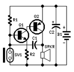
portable-alarm-for-personal-use.gif

Waiting for your soon reply ....
 

This is a very simplistic (meaning ... bad design) circuit. But here's the explanation anyway --

When SW1 opens, the bjt Q1 gets base current through R1. This turns it ON.
Now when Q1 turns on, then Q2 base gets pulled low, and it also turns on suddenly.

This means that current starts flowing through the speaker.

Since the speaker has some impedance (resistor ~ 8 ohm ? 32 ohm ? and some small inductance), there will be a sudden voltage drop across this when Q2 conducts.
This voltage will get transmitted by cap C1 back to the base of Q1, and cause it to turn off. But this is only momentary, and after a short time, the whole cycle repeats.

So at speaker, you will get an varying (square?) voltage/ current profile, and cause it to make some sound.

However note that this circuit is very dependant on the specifications of all the components, and any one component being wrong can cause it not to work properly.

I suggest you find a different project to start with - this one could prove irritating.
 
  • Like
Reactions: geo_18

    geo_18

    Points: 2
    Helpful Answer Positive Rating
Consider the switch closed Q1 base is at ground hence is turned off. Therefore Q2 is off (floating base, might be worth adding a high R base to V+ to make sure it is off?)

Now when the switch becomes open Vb of Q1 starts to rise towards V+ supply as C1 charges via R1 (note speaker is low R to V-)
At a time when Vb Q1 reaches around 0.6V then Q1 turns on which also turns on Q2.
Q2 on results in its collector going to near V+, hence max voltage across the speaker.
The positive voltage step at the speaker C1 junction also causes the base of Q1 to be pushed further positive and hence into saturation.

C1 now charges with the reverse voltage through Q2 Q1 base to emitter and R2.
When C1 is near fully charged the base current into Q1 reduces and Q1 starts to turn off which also starts to turn off Q2.
Q2 starting to turn off causes the Q2 collector to start to fall towards V- and C1 transfer this change to Q1 base making it turn off faster.
Q2 collector and hence the speaker voltage collapse to V-.
This voltage change is also is coupled through C1 to Q1 base making it fully off.

The cycle then repeats.
Critical points to this operation are R1 and the gain of Q2 with the value of C1.
I can envisage with a small value R1 or a very high gain transistor that C1 may not be able to transfer enough charge to start or maintain oscillation.

Thats how I believe it functions, but there may be better explanations.
 
  • Like
Reactions: geo_18

    geo_18

    Points: 2
    Helpful Answer Positive Rating
This is a very simplistic (meaning ... bad design) circuit. But here's the explanation anyway --

When SW1 opens, the bjt Q1 gets base current through R1. This turns it ON.
Now when Q1 turns on, then Q2 base gets pulled low, and it also turns on suddenly.

This means that current starts flowing through the speaker.

Since the speaker has some impedance (resistor ~ 8 ohm ? 32 ohm ? and some small inductance), there will be a sudden voltage drop across this when Q2 conducts.
This voltage will get transmitted by cap C1 back to the base of Q1, and cause it to turn off. But this is only momentary, and after a short time, the whole cycle repeats.

So at speaker, you will get an varying (square?) voltage/ current profile, and cause it to make some sound.

However note that this circuit is very dependant on the specifications of all the components, and any one component being wrong can cause it not to work properly.

I suggest you find a different project to start with - this one could prove irritating.

Thank you so much for your help. My project was to find a very simple circuit, so that is why I chose such a circuit.

- - - Updated - - -

Consider the switch closed Q1 base is at ground hence is turned off. Therefore Q2 is off (floating base, might be worth adding a high R base to V+ to make sure it is off?)

Now when the switch becomes open Vb of Q1 starts to rise towards V+ supply as C1 charges via R1 (note speaker is low R to V-)
At a time when Vb Q1 reaches around 0.6V then Q1 turns on which also turns on Q2.
Q2 on results in its collector going to near V+, hence max voltage across the speaker.
The positive voltage step at the speaker C1 junction also causes the base of Q1 to be pushed further positive and hence into saturation.

C1 now charges with the reverse voltage through Q2 Q1 base to emitter and R2.
When C1 is near fully charged the base current into Q1 reduces and Q1 starts to turn off which also starts to turn off Q2.
Q2 starting to turn off causes the Q2 collector to start to fall towards V- and C1 transfer this change to Q1 base making it turn off faster.
Q2 collector and hence the speaker voltage collapse to V-.
This voltage change is also is coupled through C1 to Q1 base making it fully off.

The cycle then repeats.
Critical points to this operation are R1 and the gain of Q2 with the value of C1.
I can envisage with a small value R1 or a very high gain transistor that C1 may not be able to transfer enough charge to start or maintain oscillation.

Thats how I believe it functions, but there may be better explanations.

Thank you so much for your reply, it was of great help.
 

Status
Not open for further replies.

Part and Inventory Search

Welcome to EDABoard.com

Sponsor

Back
Top