Continue to Site

Welcome to EDAboard.com

Welcome to our site! EDAboard.com is an international Electronics Discussion Forum focused on EDA software, circuits, schematics, books, theory, papers, asic, pld, 8051, DSP, Network, RF, Analog Design, PCB, Service Manuals... and a whole lot more! To participate you need to register. Registration is free. Click here to register now.

How can i improve the response of S11 parameter in antenna in FDTD code ?

Status
Not open for further replies.

sara67

Banned
Member level 1
Joined
Dec 2, 2012
Messages
32
Helped
0
Reputation
0
Reaction score
0
Trophy points
1,286
Visit site
Activity points
0
Hi guys
I wrote a FDTD code for antenna
now, when i analysis s11 parameter ,that's so bad (near zero)
firstly , i calculate V,I
secondly, i calculate Zin
then , i calculate s11=zin-zs/zin+zs
but my curev is incorrect

how can i improve that ?

plz help me if you know that , I have a little time to get the right answer
 

bad S11 means poor matching, thus reflections back to source.....
Better matching would do the job
 

Hi dear
thanks for your suggestion
but i dont know
how can apply better matching? or i can find where is problem ?
may my code was wrong ?
 

First make sure your field is calculated correctly with your FDTD code. Don't do S11 yet, you might introduce new bug during the implementation of S11.

Output your total E field at the input terminal. From the transient pulse waveform you can already tell if there is a big reflection or not.

BTW, how did you excite your antenna? Waveport? Lumped port?


Hi dear
thx for your help
how can i sure about fields are true?
i design a type of spiral antenna with FDTD
it recognize pec layer and dielectric layer and free space
i used a gaussian pulse for motivation .
and try for S11 by V,I

how can i find my wrong? in fiels or in s11 formulation or ... ?
i have not any error . so i have a mistake in my formulation , is it true?
what's your idea?
 

Spiral is not a good start for tracking issues. Can your code do a dipole antenna? Since every thing is known for dipole antenna. including field, V, I. I would suggest start from there and post your calculation results. You have not answer my question about how did you excite your structure, waveport or lumped port?
 

Spiral is not a good start for tracking issues. Can your code do a dipole antenna? Since every thing is known for dipole antenna. including field, V, I. I would suggest start from there and post your calculation results. You have not answer my question about how did you excite your structure, waveport or lumped port?

Hi
yes you are right , but i dont have enough time to exercise because i must finish it Until last month, before spiral antenna i try for a patch antenna

my type of spiral antenna is sinuous antenna
First, I wrote a code to draw it in the matlab , after that i make a function that can specify layers in my structure
my feed is in center of my structure
sorry i'm not clear on your question about waveport or lumped port?
in CST software i used waveport for feed but here i just use a gaussian pulse in central !

do i use of movie for investigative fields before s11 ?
 

may It be wrong due to boundary conditions is used?
i used ABC Mur boundry condition
ot maybe my source is wrong!?
 

Sara, lot of things might be the reason. In my personal experience, if you want to make your code work, you have to make sure that each step is 100% correct. Here is some tips from my previous debug lessons:
1. Make sure your FDTD solver is absolutely correct, you have to spend time on this. An empty cavity case is sufficient to verify it. Did you performed any test on your FDTD code?
2. After that do not doubt about field solver anymore, its done job. Focus on your ABC. The good way to test this is use a parallel plate waveguide case, PEC+PMC+ABC along X,Y,Z directions respectively. You should not observe any reflection on this case.
3. Now test if a PEC object in your FDTD can be properly handled, simply put in a PEC box or sphere and check if the EM field inside is always zero.
4. Source, according to your reply, you used a dipole source, NOTE this is completely different than lumped port, port connect two metals, dipole source does not, it simply put fields in. It looks to me that you are not exciting the problem properly, which is very likely why you did not get S11 correct. The reason you did not understand my question "Waveport or lumped port" is b/c you did not 100% understand what you are doing in your excitation.

Let me know your progress.
 

Hi dear
Thank you for the guide
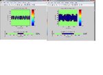
i make a movie for fields that i can see each step
my total time is 1000 but just until during 400 my fields work true after that FDTD cant specify pec and dielectric layer and over plate show with 1 color! and i can't see my shape !!
i used Superabsorption ABCs for boundry , i attach a file for you see that ,I've been using Pages 35-38 for boundry condition my code for boundry is same as it .
 

Attachments

  • best_theory_manual_FDTD_3D.pdf
    1.8 MB · Views: 382
  • 1.jpg
    1.jpg
    134.7 KB · Views: 122

Status
Not open for further replies.

Part and Inventory Search

Welcome to EDABoard.com

Sponsor

Back
Top