Continue to Site

Welcome to EDAboard.com

Welcome to our site! EDAboard.com is an international Electronics Discussion Forum focused on EDA software, circuits, schematics, books, theory, papers, asic, pld, 8051, DSP, Network, RF, Analog Design, PCB, Service Manuals... and a whole lot more! To participate you need to register. Registration is free. Click here to register now.

high voltage high speed switch

Status
Not open for further replies.

trapoe

Member level 3
Joined
Jun 2, 2008
Messages
59
Helped
11
Reputation
22
Reaction score
0
Trophy points
1,286
Activity points
1,687
hv high speed switch

I need a switch quite special to connect a 400 V to a load (50 pF // 5,6 MΩ). The rise time has to be less than 30 ns.

I would use medium power MOS, N channel. Anyone has already seen something like this ?
 

ns speed switch

50pF is not that high load. Spend some time reading data sheets and select low rise/fall time , low gate charge/capacitance mosfet. Some of the shelf gate driving IC should give you decent rise time.
 

Hi Sinisa
you're right. I've not been so clear.
I have to use two of this switch, one to charge capacitor to 250 or 400 V, the other to discharge capacitor to 0 V.
Now switches are made with a series of 2N1711 ! I want to replace with MOS and, probably, ready made driver. But I need a high voltage pulse on capacitor of no more of 50 ns, this means that I need a rise and fall time of switch shorter than 30ns, say 20-30 (less is better).
Following datasheet I can find MOS with 30 ns and driver with similar time but connected I'm not sure about total time.
And I've some doubt more: switch has an input signal very short, say 20 ns. What about propagation time? Do they open and close in few tenth of ns.
In this circuit all components works to their limit and I would like to know if someone has already some experience to share because I don't like so much to make the circuit and see that it's impossible to achieve the goal.

P. S. your moving avatar is very nice but previous was much more "human" :D:D
 

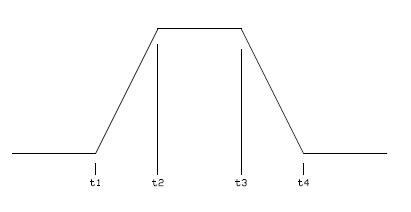
Just to clarify: what is 20ns in your input pulse? t1-t4 or t2-t3?
40_1223913653.jpg
 

It could be 50 % rise to 50 % fall. This is jut to give you an idea. To have a trapezoidal wave on capacitor of 40 ns or less I close the first switch (to 400 V) then I open it. Then after a while I close the second switch to discharge the capacitor.
To achieve a duration of high voltage pulse on capacitor of 40 ns I have to open and close the first switch in less than 40 ns, say 20 ns. This is the duration of the input pulse of the driver of the first switch.
Hope this will be clear.
 

That should not be a problem. There is going to be propagation time through circuit, but in my understanding of your problem, thet should not be a problem. You are mostly concerned with rise/fall times, and you can do that by aplying signal from driver that has high current capability. Put resistor in series with gate, but also bypass same resistor with small capacitor to offset gate capacitance. You tune this to get optimum performance, sort of like when you tune oscilloscope probe to get square wave shape without ringing.

If you have problems obtaining suitable gate driver, **broken link removed** can be used. You could use this circuit with corrected voltages not to exceed Mosfet rating. You will need this circuit on both fets. You can create suitable delays for driving circuits with your TTL circuits and tune it untill you get just sufficient dead time. Small overlap will probably not affect mosfets other then slightly increasing heat and power cinsumtion. Larger overlap will cause problems.

Other option that is probably easier is if you create A class output with current source from +400V and pull it down with N mosfet. You could use single discreete solution or some high current gate driver with sufficient speed. Again, delay is not crucial as pulse will have same rise fall times and duration, it will just be shifted in time.
 

HI Sinisa
Thank you for useful link to discrete driver circuit ... and for your patience.

My doubt about relation between propagation time and maximum frequency and minimum period.
You're thinking at driver (or any device) as something like a "delay line". If you change an input the output will change after a delay similar to propagation time. No matter how quickly you change input. This lead to a maximum switching frequency limited only by transition time in logic circuits.

My opinion is that you can't change input before output is changed, so you have to wait for the propagation time. Then the minimum period will be the sum of propagation times.
This seems more similar to what I remember. Think at 74HC CMOS logic. Typical transition times at Vcc = 5 V are around 5 ns this means maximum frequency of 100 MHz.
Typical propagation times are more than 10 ns, if I'm right this lead to maximum frequency of less than 50 MHz. More realistic.

Current source from 400 V. If I understand what you mean to charge 50 pF to 400 V in say 20 ns I need 1 A. Pulling down 1 A from 400 V give 400 W.

Finally. If a driver with say 30 ns rise time is connected to a MOS with 30 ns rise time I can't have total rise time of 30 ns. I'll have something more, probably something like a quadratic sum, say 45 ns. That's too much for me.

Final question: overdriving bjt can improve speed. Is the same with MOS ?
 

Final question: overdriving bjt can improve speed. Is the same with MOS ?
You can see from MOSFET datasheets, that above a gate-source-voltage of e. g. 10 V, the on-resistance respectively the drain current is nearly unchanged. Overdriving effectively doesn't speed-up switching beyond a certain level.

But's it's no problem to achieve e. g. 5 ns and less rise-time at the gate with fast bipolar transistors. The switch behaviour is almost defined by the MOSFET properties then. The achievable rise-time depends on the MOSFET technologie, ranging from below 5 ns with fast DMOS transistors (unfortunately, there's only a small type choice and many devices have been discontinued, e. g. from Supertex) to about 20 to 50 ns with standard small-signal MOSFET.

You also made some considerations regarding switching frequency, but I didn't exactly understand it's relevance for your application, cause you didn't specify a pulse repetition rate. To my opinion, it mainly matters regarding average power consumption. The 400 W pulse power are sounding heavy, but don't affect the devices much in case of a low pulse frequency.
 

I don't know what you mean by overdriving... If you exceed maximum Vgs, I don't think you could gain any speed.
Let's consider Ixys **broken link removed**. Data sheet states td(on)=15ns(typ.) Conditions under which was tested are 20\[\Omega\] gate resistor and 10V pulse to achieve current of 3.6A (Id25)
When you take into account gate capacitance, what Vgs is required to get to those 3.6A, you will come close to those 15ns. Now if your circuit is well done and you dont have undesired oscillations, you can bypass resistor with capacitor creating RLC circuit with lead inductance, gate capacitance lead resistance... You want to tune gate circuit but first you have to make sure layout, decoupling and everything else is way it should be. You have to treat design as dealing with RF. Once you achieve that Vgs rises much faster than desired 10ns, you will see what kind of performance you could squeeze out of that transistor.


As for 400W, you should be concerned with maximum energy rating of transistor. 400W you talk about should be supplied by decoupling capacitors, not the PSU.(given that frequency of the pulses does not have to be to high)


Just to add, if you want to achieve really fast, HV pulses, BJT in avalanche mode could give you sub ns pulses. You have to be aware that whole signal path from source to the load has to perform at those frequencies.

My opinion is that you can't change input before output is changed, so you have to wait for the propagation time. Then the minimum period will be the sum of propagation times.
This seems more similar to what I remember. Think at 74HC CMOS logic. Typical transition times at Vcc = 5 V are around 5 ns this means maximum frequency of 100 MHz.
Typical propagation times are more than 10 ns, if I'm right this lead to maximum frequency of less than 50 MHz. More realistic

Consider 50 inverter gates connected in series. Is maximum frequency you could run through those gates 1/(tp*50)?
 

you can bypass resistor with capacitor creating RLC circuit
I don't see a particular purpose of this circuit in driving MOSFETs (ot capacitive loads in general). You could use zero ohm resistance as well. The usual way is to reduce the gate resistor until the intended gate rise time is achieved or the oscillations get inacceptable (in case of a bad layout).
 

I found it easier to tune with trimcap than trimpot. Maybe due to added inductance of trimpots I had available.
 

Use a high voltage RF mosfet with a high speed driver
 

Status
Not open for further replies.

Similar threads

Part and Inventory Search

Welcome to EDABoard.com

Sponsor

Back
Top