Continue to Site

Welcome to EDAboard.com

Welcome to our site! EDAboard.com is an international Electronics Discussion Forum focused on EDA software, circuits, schematics, books, theory, papers, asic, pld, 8051, DSP, Network, RF, Analog Design, PCB, Service Manuals... and a whole lot more! To participate you need to register. Registration is free. Click here to register now.

high swing current mirror?? please help me ..

Status
Not open for further replies.

alicia8283

Junior Member level 2
Joined
Mar 3, 2005
Messages
21
Helped
2
Reputation
4
Reaction score
1
Trophy points
1,283
Activity points
1,436
high swing cascode current mirror

hi all,

I am beginner for analog design. Can somebody help me to explain the difference between that two circuit that i uploaded?

55_1157419276.gif


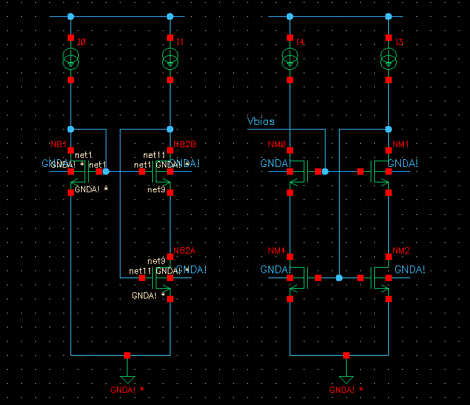
the right hand side is the normal high swing cascode current mirror that i normally read, but i don very understand for the left hand side's current mirror.

i guess that's also high swing current mirror? But will it caused mismatch to connect in this way? how should i derive the equation for it?

thank you very much for your help :)
 

high voltage current mirror

Where do you get the bias voltage in the right side? I think that the left side diode connected transistor can provide this voltage
 

high swing current source

ya.. the Vbias i get it from others mirror circuitry..
but the question now is i don understand how should analyse the circuit at left hand side .. and need the derivation for it.. :)
 

high swing current mirror

HI all ,

Left hand side is the first order high swing cascode mirror . U can see the bias for the top transistor and the second bias is provided by that ckt itself.

Ckt on the right side is used for better matching and to avoid the bodf effect faced by the top transistor.here u will have more contraints in the deisgn as u have to see all the four transistors are in saturation
 

    alicia8283

    Points: 2
    Helpful Answer Positive Rating
current high swing

again the difference in vds drop is also accounted and hence very perfect matching is obtained
 

current mirror mosfet

the right side circuit may be not completely.In fact ,it is necessary to bias them with a diode transistor.you can refer to the martin's book.
 

diode connected transistor saturation equation

thats right shake but the currents will be matched between the right and left arm as the feedback will make sure that the currents are equal (proportional) I am quite sure that it is 100% matching and we need to tweak the bias to have the magnitude of current as the desired one.
Correct me if I am wrong.
 

diode connected transistor saturation

The left one is not a current mirror.
This is just a diode connected NMOS, with a cascode to keep the drain voltage constant. There is nowhere current mirrored.

The left one is just a way of biasing the cascodes in the right one. (which is a normal high swing current mirror)

br, Jef
 

high-swing current source

The left one is part of a high-swing cascode mirror.

The right one is a cascoded mirror, but lacking the bias generation circuit for the cascode transistor. So, both circuits aren't complete.

In the left circuit NB2A programs the current, and NB2B is a cascode device that improves matching. The gate voltage of NB2A is the mirror programming current, and the gate voltage of NB2B must be connected to some circuit that generates a vbias for it.

NB1 is the circuit that generates this bais voltage for the cascode.
Assuming that the mirror transistors are identical, just make the L of NB1 between 1/4 and 1/5 of the L of NB2 and you will generate a vbias that keeps drain voltage of NB2A just above the saturation limit.

This circuit is described in the book by Johns and Martin, btw. Solve the square-law equation for NB1 in terms of the size W/L of NB2 and the vdsat of NB2 and you'll get this result.
 

vds of a diode connected transistor

really thank you everybody for the explanation :)
 

high swing current mirrors

idea to make well matched current mrrors is simple:
ids=B(Vgs-Vth)^2(1+λVds)
make Vgs (it is normallly done when you connect gates and sourcea) and use matched mosfets(important matching is for mosfets near gnd) with same Vds (by proper circuit configuration and biasing). For matching L has to be high enough ...say 4-10xLmin... For high output resistance use cascode...For high swing design bias mosfet that keps at vds voltage level slightly higher than vdsat...

Left circuit is not current mirror because all points have low impedance (diode connected mosfets). It can be biasing for current mirror.

At the current mirror output you should put resistor, not current source...
Dont make bias as voltage generator, use diode connected mosfet and current source instead(it is easier... especially when you cgange temperature...)....size should be scalable to mirror mosfet but avoid factor more than 4...
 

use of diode connected mos in current mirrors

Why are there two ideal current sources? Which one is the reference current?
 

low swing cascode resistor

I thik ZUZUZU i right
you have a big problem in your shematic
ther is a conflict between the 2 ideal current sources

At input of the current mirror it is logic to place an ideal current source. At output you can place a constant voltage source or a resistor as a load, but never a current source!

good luck
 

Status
Not open for further replies.

Similar threads

Part and Inventory Search

Welcome to EDABoard.com

Sponsor

Back
Top