Continue to Site

Welcome to EDAboard.com

Welcome to our site! EDAboard.com is an international Electronics Discussion Forum focused on EDA software, circuits, schematics, books, theory, papers, asic, pld, 8051, DSP, Network, RF, Analog Design, PCB, Service Manuals... and a whole lot more! To participate you need to register. Registration is free. Click here to register now.

High side current sensing: Rsense placement and vias.

Status
Not open for further replies.

JMG

Member level 3
Member level 3
Joined
Sep 27, 2005
Messages
66
Helped
0
Reputation
0
Reaction score
0
Trophy points
1,286
Visit site
Activity points
1,908
I'm creating a basic ~90W DC/DC converter using the LM3904HV driver. Input is 48v to 60V, output is 29v to 31V @ 2.8A MAX.

Regarding placement of the sense resistor, trace length to the FET gate and Drain, and vias within the sensing net: The resister is as close to the driver as practical (about 0.500" net length) but this means I'd have to run a few vias and about a 1.50" net length to the Drain. Is this acceptable? There would be no vias between the resistor and the driver, just the drain and the resistor.

My other question is how long is too long to run a net to the gate from the driver. Currently this would be around 2.25" with 2 vias. Fsw is 100KHz.

Thanks.
 

I think you mistyped the mpn, LM3904HV doesn't show any matches when searching.
 

Okay, I see now.

The length of the sense traces from Rsense to the CS pins is not very critical, since those pins are high impedance. What is critical is the loop formed by the input bypass capacitor, Rsense, the catch diode, and the ground plane. That loop must be kept as small as possible since it must carry discontinuous currents. For good gate drive, the loops formed with the ground and Vin pins of the chip and the gate drive pins should also be kept small. For Fsw of 100KHz, a couple inches of length is a lot, but what it really comes down to is loop area. IMO you should try to keep all of those critical loops to be maybe one or two square centimeters at most.
 

I can keep the rsense, i/p caps, catch diode all very close together but then that creates 2 issues. 1: the rsense to drain trace has to go under the ground plain where those components connect and 2: this increases the size of the plain for the catch diode, fet source and inductor input.

I will see if I can get a screen grab of the current layout.
 

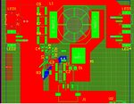
dcdc1.jpgpcb2.jpg

C1 and C2 are the input caps, D1 is the catch diode, R3 is the sense resistor.. This area is decently tight. Where things get interesting is the R3 via to M1 drain vias plain on the bottom layer (in blue.) The total net length from R3 pad to M1 pad is 0.853". Sure, I can tweak it down 0.050" - 0.100" but its not going to get down to being pretty short with the cureent layout configuration.

Another concern is the M1 source to inductor plain. It needs to be large enough to carry the current and dissipate heat but not too large as to create inductance problems.
 

Another concern is the M1 source to inductor plain. It needs to be large enough to carry the current and dissipate heat but not too large as to create inductance problems.
Why should you expect "inductance problems" when connecting a rather small trace inductance in series with a large inductor? It's true that trace inductance is critical for some connections, but not for the present one. M1.source/R3 to output capacitors is e.g. much more critical.
 

Pulled that concern directly from the datasheet. I agree with you - I've never made much effort to decrease this trace size, in fact I've always made it large to enable much better cooling of the fet.
 

Why should you expect "inductance problems" when connecting a rather small trace inductance in series with a large inductor? It's true that trace inductance is critical for some connections, but not for the present one. M1.source/R3 to output capacitors is e.g. much more critical.
That FET inductance isn't directly in series with the inductor, it forms a junction with the catch diode, and that's where the high frequency commutation takes place. So of course inductance in series with the FET or diode will matter a lot.

As it is, the critical input loop isn't very big, but it could be better my moving R3 to the top layer and putting it directly between the input caps and the source. That will probably mean you have to route the sense traces on the bottom layer, but that's much better than running the sense current itself underneath.
 

That is a lot better. But you should fix your CS traces to connect directly at the R3 terminals. Also you may want to shrink the size of the switching node, if it's too large it will radiate lots of interference.
 

I'm concerned about heat in that fet. The ambient temperature is going to be up to 60 deg C. There isn't enough space in the enclosure for a heat sink so the only thing I have is a copper plain.

dcdc3.jpg
 

Status
Not open for further replies.

Part and Inventory Search

Welcome to EDABoard.com

Sponsor

Back
Top