Welcome to our site! EDAboard.com is an international Electronics Discussion Forum focused on EDA software, circuits, schematics, books, theory, papers, asic, pld, 8051, DSP, Network, RF, Analog Design, PCB, Service Manuals... and a whole lot more! To participate you need to register. Registration is free. Click here to register now.
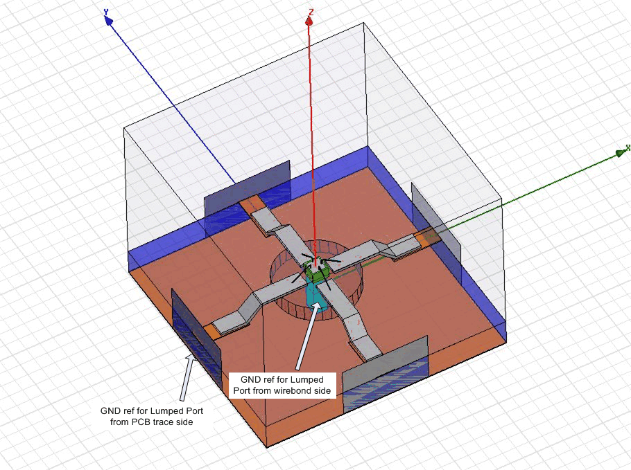
Here the package model. I have drawn the blue box (pec material) to make ground reference for the lumped ports from wirebond sides. The HFSS simulation results in good agreement with Q3Dextractor results. But are there another way to simulate the package without the blue box?
I did not define any infinite ground planes. If I do this the infinite ground plane (on chip) will cross other objects of the package 3D model...
It seems to me, that I solved the problem I am using export to fullwave SPICE now. In this way I can define arbitrary ground reference for ports and effectivly use it in circuit simulator. The results from circuit simulator with the fullwave SPICE model are meaninfull so I think it is ok.
This site uses cookies to help personalise content, tailor your experience and to keep you logged in if you register.
By continuing to use this site, you are consenting to our use of cookies.
") I am using export to fullwave SPICE now. In this way I can define arbitrary ground reference for ports and effectivly use it in circuit simulator. The results from circuit simulator with the fullwave SPICE model are meaninfull so I think it is ok.
I am using export to fullwave SPICE now. In this way I can define arbitrary ground reference for ports and effectivly use it in circuit simulator. The results from circuit simulator with the fullwave SPICE model are meaninfull so I think it is ok.