Continue to Site

Welcome to EDAboard.com

Welcome to our site! EDAboard.com is an international Electronics Discussion Forum focused on EDA software, circuits, schematics, books, theory, papers, asic, pld, 8051, DSP, Network, RF, Analog Design, PCB, Service Manuals... and a whole lot more! To participate you need to register. Registration is free. Click here to register now.

Help with H-bridge inverter please

Status
Not open for further replies.

binaryninja

Member level 3
Joined
Nov 11, 2010
Messages
65
Helped
2
Reputation
4
Reaction score
2
Trophy points
1,288
Activity points
1,945
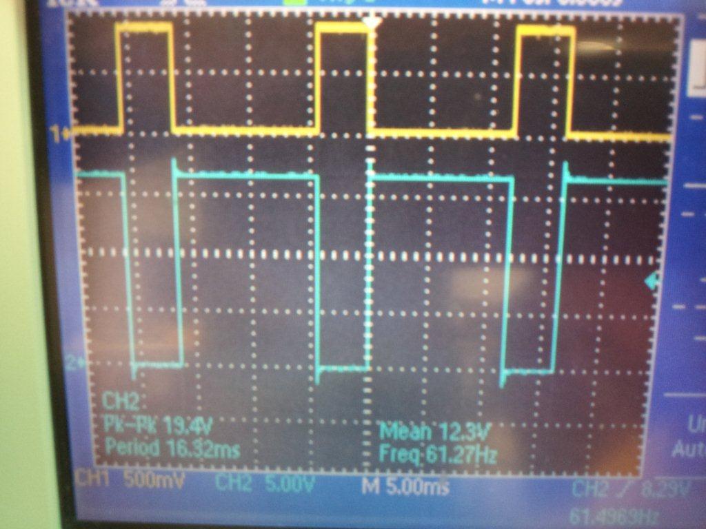
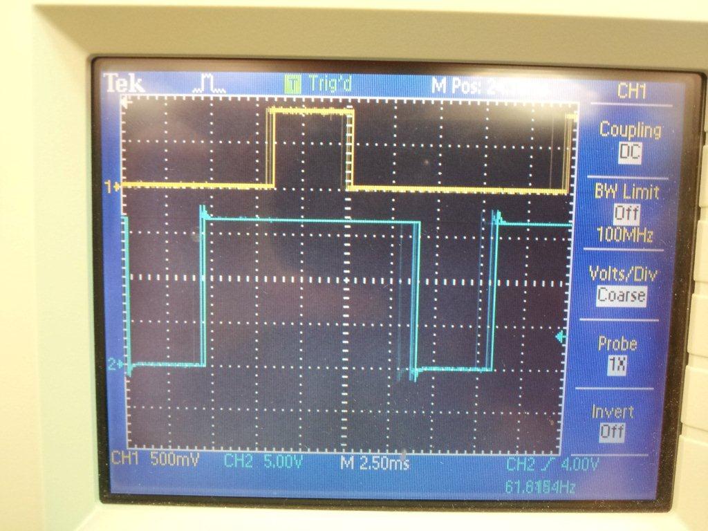
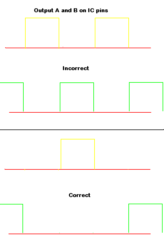
Howdy, I am trying to use a TI UCC28089 PWM controller, that has a modified square wave H-bridge inverter schematic on page 11. I have built and tested the circuit, driving it with 155V. The circuit works just fine without a load. With just a 7.5W bulb as the load the circuit starts whining a little then eventually fails. The high side transistor on the left side keeps burning up. I needed this exact spec (110VAC/60Hz, modified square wave) so I thought why not give it a go. My overall power goal is 200W.

This is my first H-bridge (inverter) and I have tried a few things but I'm not sure what needs to be done. I need a H-bridge inverter that works well at high voltage/current. Can you suggest any modifications and/or alternative circuits that will do the job? Thanks!

I know there are several posts on H-bridges, I have been looking through them. I would like to continue with the UCC28089, I don't think the controller is the problem but it could be.
 

Attachments

  • (U8) ucc28089.pdf
    563.8 KB · Views: 169
Last edited:

You mean upper left FET is getting destroyed? Check related components which can cause trouble. MPSA42 not switching probably. 12V should be present on 4.7uF capacitor. SG3524 is similar ic with adjustible duty cycle. 6800pf capacitor is necessary in lower leg to avoid shoot through.
 
Last edited:
I recommend using MOSFET instead of transistor for high power ratings... I have done using MOSFETs and it works fine...
can u give details of your triggering circuit coz u have to confirm whether u have created a dead zone or not....
 
You mean upper left FET is getting destroyed?
No, the fets are fine. I haven't destroyed one of those yet. It is the MPSA42s that keep burning up. I have increased the 200 Ohm resistors to 30K, and placed another resistor between the charging diodes and the collectors. I have also increased the base resistance to 820 Ohms. They still cook, even at light loads.

I recommend using MOSFET instead of transistor for high power ratings
I am going to try this. Although, I have seen a couple of other inverter designs that use the MPSA42 for the high side switching. It is rated for 300V and 500mA.

can u give details of your triggering circuit
I really just pulled the circuit straight from the datasheet. On the scope, the modified square wave looks good. Once a load is applied, the switching continues but the transistors get super hot and eventually die.

Is there anything that can be done to decrease the amount of current through these transistors that I haven't already tried? Eventually, I need this circuit to handle 200W. What can be done to make it more robust and stable? I'll see if replacing the transistors with fets helps.
 

It is left side transistor burning and left half bridge and right half bride are identical, so it is obvious that there is something wrong on left side construction. If we analyse the circuit around MPSA42, the only load is 200 ohm resitor and it is active when voltage decreses below 12V and a current of 50mA. So there is no obvious reason for the transistor getting destroyed except one. When load is attached, the load current is passing through this trasistor. This could happen when lower left FET is not turning on in time. When right upper FET is in on state, current will pass through it and ten to load and when lower fet is not in on state, the current path will be through the protection diode connected between gate and source of upper left FET and through the upper left MPSA42 (which is on) to ground.
The gate resistance of 200 ohm and 6800pF capacitor make a time constant.
I have increased the 200 Ohm resistors to 30K
This is going to worsen the case. Confirm all resistors and capacitors are according to values in schematic. On lower left FET's gate, if 200 ohm resistor value is higher or capacitor value is higher, this condition will happen. Interchange the left and right output of ic to confirm ic is ok. Change the value of both 6800pF capacitor to 1000pF(102n) and see the result. Gate series resistance is 200 ohm(180 to 220 ohm), base resistance 47-100 ohm
Another very important point to consider is that if the value of Rs(current sense resistor) is too high, that is voltages developed across it is greater than 0.5V, load current will flow that small transistor and destroy it. A circuit modification will help. Put a series resistor of near 10 ohm between collector of MPSA42 and to the point where gate of FET and 200 hm resistor attach. Another modification will be disconnecting emmiters of MPSA42 and connecting to common point of lower FETs sources.
 
Last edited:
Hi Alterlinks, thanks for the analysis.

there is something wrong on left side construction
Originally, I thought it was only one side, apologies.

I guess I wasn't clear enough in my latest post. This is happening on both upper sides, both MPSA42s get cooked with a load. I know all legs of the H-bridge need to be balanced. I only increased the 200 Ohm resistors on the high sides, to try and decrease the power dissipation of the BJT. I know if the lower legs have larger resistances on the gates of the fets it will slow down their switching.

Thanks a lot for the current path explanation, I couldn't figure out why this was happening. All the math says otherwise, and the BJTs should be okay. It makes sense that it only happens when there is a load now. To repeat what you say, the lower fets are turning on too slowly, so slow that the load current is getting dissipated through the BJTs to ground.
 

As the circuit is supposed to be correct (it is included in aplication note), the posibility of Rs value being too high is more. It should not be more than 0.2 ohm.
 
Thanks so much for your help. The BJT overheating issue is solved! The load current was taking the wrong path. I replaced my Rs and removed the 6800pF caps.

Now, I have a new problem that I was hoping you could help me with. I went all the way up to a 75W load and the AC voltage begins to drop to ~102VAC. The DC supply voltage does stay up to around ~150V which is still enough for 110VAC. With a 150W load the DVM doesn't even pick up an AC voltage, and the DC supply to the H-bridge stays at ~155V. Any ideas as to what could be happening at the bigger loads?
 

With a 150W load the DVM doesn't even pick up an AC voltage, and the DC supply to the H-bridge stays at ~155V.
You mean at 150 watts, there is no output. If pin4(current sense) is picking some spike pulses, it can shutdown ic and then take more than a second to restart but again a pulse will retrigger.
CS: Connect the current sense device to this pin. A voltage threshold of 0.725 V triggers a shutdown sequence.An over-current fault triggers an immediate shutdown. After the fault clears, a total of 64 oscillator cycles are required for an entire soft start sequence to occur. First, the outputs and SYNC are kept OFF for at least 56 oscillator cycles.Next, after one or two SYNC pulses, the soft start progressively increases the output duty ratio over the next five to seven oscillator cycles.
It is only a matter of adjusting resistor network on this pin#4. A small capacitor like 6800pF between cs pin and ground pin#5 will also help.
 
Last edited:
Well, unfortunately it isn't the CS that is killing the H-bridge. I have tied the CS pin to VSS with the same results.

The same thing keeps happening, which is the left side MPSA42 breaks down and shorts the gate of the high side fet to ground. This happens only at higher loads, specifically once I get near 90W. I feel like this is a driving issue, possibly shoot through, like the lower fet isn't coming on fast enough for the current to have a path to ground. Like what you were saying before. I have attached a picture of the gates of the two left side fets. The yellow line is the low side. It is on for a shorter time than the high side, is this correct? Shouldn't the two have equal on/off times?


---------- Post added at 12:05 ---------- Previous post was at 11:23 ----------

Here is a pic of the fets that are on at the same time. Once again, can someone please tell me if this is correct? I thought that they were suppose to be on for the same amount of time and the deadtime was the duration that neither was on. Thanks!


Hi,
Is there any snubber CAP on your 155VDC close to the fets?(there isn't any on page 11)
If not you need one at least. 100n/200v MKP or similar.
 

The inputs of upper FETs are inverted due to MPSA42 and resitor action.So upper pic is ok . It should look the same on both half bridges. Duty cycle and frequency is practically ok inthis scope trace pic.
I thought that they were suppose to be on for the same amount of time and the deadtime was the duration that neither was on.
Here the deadtime is the duration that both lower or both upper are on.
For step sine wave,
5_1322056899.png
 
Last edited:
Is there any snubber CAP on your 155VDC close to the fets?
No, I don't have any snubbers on the fets of the H-bridge.

Here the deadtime is the duration that both lower or both upper are on.
Thanks for the diagrams. Okay, so I'm a little confused. The PWM outputs from the IC, do have the appropriate deadtime. They look like your "correct" diagram. In the second pic the blue line is the upper fet, so this wave is also inverted. Then there is a duration of time in the second pic when both fets are off, and this would also be correct, right?

So, if my timing and switching are correct, then why is the high side driver MPSA42 getting burned up at a higher load? When I watch the scope with the higher load that causes the H-bridge to fail, there are sharp descents and then nothing but wacky lines that don't look like anything. Turn the load off and it goes back to normal. What could be causing the H-bridge to simply just not work at a higher load (besides CS)? The controller still outputs the PWM signals, but it's like the H-bridge can't handle the load current even though everything is well within the ratings. The frequency ratings are all good as well, so it's not like my switching components aren't fast enough. Could it have anything to do with my boost capacitor? Is there anything I can add to the circuit to help with possible transients? I will try adding snubber circuits.
 

32_1322070188.jpg

This is the right switching for half bridge. Blue line , inveted, input for upper FET and yellow is input for lower FET. Similar should be for other half hbridge. The second pic you posted and refering to, is kind of strange. There is time when both fet are on. If this is so, FETs should have been burned in an instant. As both upper and lower FET is driven by same driving pulse with a inverter in between for upper FET, this cant be, You are mixing left and right, i think. Dead time is when both upper FETs are on. The actual deadtime is provided by 6800pF capacitors, making a small delay while lower FET is turning on after upper FET turns off but this may cause stress to MPSA42 transistor as early dicussed.
 
Last edited:
Status
Not open for further replies.

Similar threads

Part and Inventory Search

Welcome to EDABoard.com

Sponsor

Back
Top