honeyazwan
Newbie level 1
telescopic design
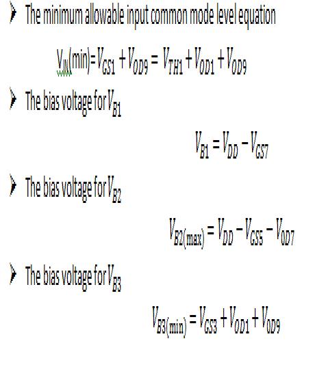
Calculation for the input common mode level and the bias voltage V_B1 , V_B2 and V_B3. It must be chosen so as to allow maximum output swings.
netlist for the design using Hspice
********** AOL, GBW, PM SETUP **********
Vin1 0 N1 dc 1v
Vin2 N2 0 dc 1v ac 1
X1 N1 N2 Vout2 N3 0 telescopic_amp
.OP
.AC DEC 10 1Hz 100MegHz
********** SR & TS SETUP **********
*Vin2 N2 0 PWL (0, 1.4V, 10us, 1.4V, 10.01us, 2.4V, 30us, 2.4V, 30.01us, 1.4V, 40us, 1.4V)
* X1 Vout2 N2 Vout2 N3 0 telescopic_amp
*.OP
*.TRAN 0.1ns 50us
********** ICMR SETUP **********
*Vin2 N2 0 dc 1v
*X1 Vout2 N2 Vout2 N3 0 telescopic_amp
*.DC Vin2 0 2 10mv
********** OCMR SETUP **********
*Vin2 N2 0 dc 1v
*VDD N3 0 2.5
*X1 N1 N2 Vout2 N3 0 telescopic_amp
*R1 N1 Vout2 10Meg
*R2 N3 N1 1Meg
*.DC VDD 1.4 1.9 0.1
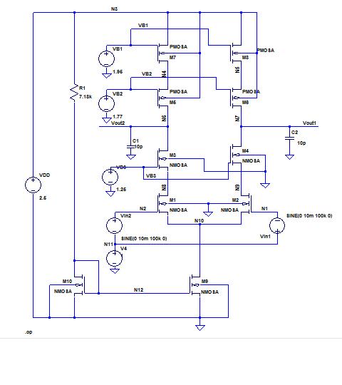
.subckt N1 N2 Vout2 N3 0 telescopic_amp
* O=GND
VDD N3 0 2.5
C1 Vout2 0 10p
C2 Vout1 0 10p
Rref N3 N12 7.18k
VB1 VB1 0 1.95
VB2 VB2 0 1.77
VB3 VB3 0 1.25
*mod d g s b modName L=a W=b
M1 N8 N2 N10 0 NMOSA l=1.8u w=38u
M2 N9 N1 N10 0 NMOSA l=1.8u w=38u
M3 Vout2 VB3 N8 0 NMOSA l=1.8u w=10u
M4 Vout1 VB3 N9 0 NMOSA l=1.8u w=10u
***pmos load***
*mod d g s b modName L=a W=b
M5 Vout2 VB2 N4 N3 PMOSA l=1.8u w=124u
M6 Vout1 VB2 N5 N3 PMOSA l=1.8u w=124u
M7 N4 VB1 N3 N3 PMOSA l=1.8u w=124u
M8 N5 VB1 N3 N3 PMOSA l=1.8u w=124u
***current mirror*****
*mod d g s b modName L=a W=b
M9 N10 N12 0 0 NMOSA l=1.8u w=6.02u
M10 N12 N12 0 0 NMOSA l=1.8u w=6.02u
.options list node post
.option post = 1
.end
result:
from the result itself, only M5, M6 and M11 in saturation..what suppose i redesign to make all the transistor in saturation. i already varies the vod for PMOS load to be larger but it doesnt work...plz help me..=.=
Calculation for the input common mode level and the bias voltage V_B1 , V_B2 and V_B3. It must be chosen so as to allow maximum output swings.
netlist for the design using Hspice
********** AOL, GBW, PM SETUP **********
Vin1 0 N1 dc 1v
Vin2 N2 0 dc 1v ac 1
X1 N1 N2 Vout2 N3 0 telescopic_amp
.OP
.AC DEC 10 1Hz 100MegHz
********** SR & TS SETUP **********
*Vin2 N2 0 PWL (0, 1.4V, 10us, 1.4V, 10.01us, 2.4V, 30us, 2.4V, 30.01us, 1.4V, 40us, 1.4V)
* X1 Vout2 N2 Vout2 N3 0 telescopic_amp
*.OP
*.TRAN 0.1ns 50us
********** ICMR SETUP **********
*Vin2 N2 0 dc 1v
*X1 Vout2 N2 Vout2 N3 0 telescopic_amp
*.DC Vin2 0 2 10mv
********** OCMR SETUP **********
*Vin2 N2 0 dc 1v
*VDD N3 0 2.5
*X1 N1 N2 Vout2 N3 0 telescopic_amp
*R1 N1 Vout2 10Meg
*R2 N3 N1 1Meg
*.DC VDD 1.4 1.9 0.1
.subckt N1 N2 Vout2 N3 0 telescopic_amp
* O=GND
VDD N3 0 2.5
C1 Vout2 0 10p
C2 Vout1 0 10p
Rref N3 N12 7.18k
VB1 VB1 0 1.95
VB2 VB2 0 1.77
VB3 VB3 0 1.25
*mod d g s b modName L=a W=b
M1 N8 N2 N10 0 NMOSA l=1.8u w=38u
M2 N9 N1 N10 0 NMOSA l=1.8u w=38u
M3 Vout2 VB3 N8 0 NMOSA l=1.8u w=10u
M4 Vout1 VB3 N9 0 NMOSA l=1.8u w=10u
***pmos load***
*mod d g s b modName L=a W=b
M5 Vout2 VB2 N4 N3 PMOSA l=1.8u w=124u
M6 Vout1 VB2 N5 N3 PMOSA l=1.8u w=124u
M7 N4 VB1 N3 N3 PMOSA l=1.8u w=124u
M8 N5 VB1 N3 N3 PMOSA l=1.8u w=124u
***current mirror*****
*mod d g s b modName L=a W=b
M9 N10 N12 0 0 NMOSA l=1.8u w=6.02u
M10 N12 N12 0 0 NMOSA l=1.8u w=6.02u
.options list node post
.option post = 1
.end
result:
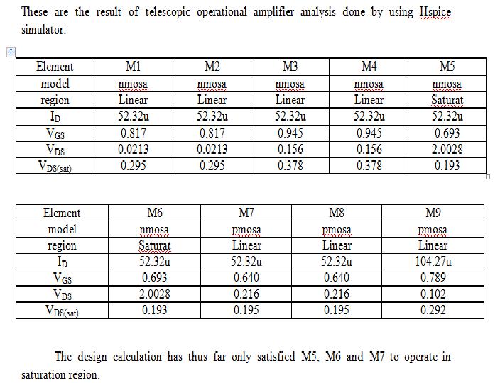
from the result itself, only M5, M6 and M11 in saturation..what suppose i redesign to make all the transistor in saturation. i already varies the vod for PMOS load to be larger but it doesnt work...plz help me..=.=