Continue to Site

Welcome to EDAboard.com

Welcome to our site! EDAboard.com is an international Electronics Discussion Forum focused on EDA software, circuits, schematics, books, theory, papers, asic, pld, 8051, DSP, Network, RF, Analog Design, PCB, Service Manuals... and a whole lot more! To participate you need to register. Registration is free. Click here to register now.

Help with 4051B multiplexer circuit

Status
Not open for further replies.

RedShiftJames

Newbie level 3
Joined
Mar 24, 2014
Messages
4
Helped
0
Reputation
0
Reaction score
0
Trophy points
1
Activity points
39
Hello EDA, I am an A2 Electronics student and I need help with my multiplexer circuit.

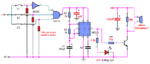
Attatched is a screenshot of my circuit in Circuit Wizard. Basically it's a bike alarm with a combination to turn it off. The combination to turn output 6 on turns the alarm off, as output 6 is grounded. This all works in the simulation but when I came to build it IRL, I had a few problems.

https://obrazki.elektroda.pl/5211735100_1395668852.png

When I turn the input switches on for inputs A, B, and C, the outputs don't work as intended. There is no "defuse" combination; the led I used to test the output just glows brighter the more switches are turned on.
Also, the chip gets hotter and hotter as soon as I connect the 9V battery to the 9V and 0V rails. This heat eventually creates resistance so the testing LED just gets dimmer over time, to the point where you can't see the glow at all.

Does anyone know where I've gone wrong here? Does it have something to do with the fact that I connected 7 multiplexer outputs together?
 

The inputs S1,2,4 are left floating when the switches are turned off. CMOS inputs must not be left in that condition.
Connect a resistor from each of those inputs to 0V (GND). The value is not critical, rather high is ok for reduced consumption, but too much can fail to force a low level; 100 kohms would be ok.
Don't forget to connect supply for the 4051 (pin 8 at 0V and pin 16 at 9V).
Regars

Z
 

    V

    Points: 2
    Helpful Answer Positive Rating
You have the CD4051 supplying power to the 555 and to the output transistor. But its on-resistance is too high to power anything.
Instead, the CD4051 can be used to reset or allow the 555 to function then the 555 can turn on and turn off the output transistor.

If the current used by the ordinary 555 is too high when it is reset then replace it with a Cmos 555 (LMC555, TLC555 or ICM7555).
 

    V

    Points: 2
    Helpful Answer Positive Rating
Thanks for the responses, guys! I'll try using these tips on Wednesday and I'll update on whether it worked. :)
 

Hmmm, it's not worked, so I decided to build my own multiplexer using logic gates. However, when I connect it to the Astable input, it doesn't power it. I just know that what I've done wrong is something really simple and dumb, but I have no idea why it's happening.

https://obrazki.elektroda.pl/6772911600_1396429148.png

I just find that rather than trying to use an IC I don't fully understand, I would use logic gates instead.
 

Again, you have your Cmos inputs floating so that they never go to a logic low. I added 100k resistors to the inputs to pull them low when the switch is opened.
The output current of Cmos logic ICs (like your CD4023) is very low so I increased the value of the resistors from the output of the 555, used a low current piezo transducer instead of a high current speaker, disconnected the load for the transistor from the CD4023 and instead powered it directly from +9V and added supply bypass capacitors.
 

Attachments

  • multiplexer.png
    multiplexer.png
    20.6 KB · Views: 96
Ace, adding those resistors worked, I added another for the last NAND input as well. I didn't bother with the capacitors, as the circuit worked when I changed R1 on the astable to a 10K and then powered the buzzer from 9V.

I had a funny moment where it wasn't working because I was covering the hole on the buzzer (I was using a buzzer from the start by the way, not a loudspeaker like my diagram appeared to have) and it was going crazy, so I tried a bunch of stuff but then decided that if my classmates didn't want to hear loud noises, they would just have to deal with it. Then I let the thing buzz with completely uncovered and that was it! It was working! :)

Thank you both for your help!!
 

Ace, adding those resistors worked, I added another for the last NAND input as well.
Where did you add a resistor?Tthe 3-inputs NAND has resistors I added on two of its inputs and the Cmos inverter drives its 3rd input high or low so another resistor is not needed.

I didn't bother with the capacitors
ALL electronic circuits need a capacitor to ground on their power supply terminals. The datasheet for the 555 shows TWO capacitors to prevent it from causing interference to circuits using the same power supply because it draws 400mA (!) each time its output switches. Your poor little 9V battery NEEDS a capacitor.
 

Status
Not open for further replies.

Similar threads

Part and Inventory Search

Welcome to EDABoard.com

Sponsor

Back
Top