Continue to Site

Welcome to EDAboard.com

Welcome to our site! EDAboard.com is an international Electronics Discussion Forum focused on EDA software, circuits, schematics, books, theory, papers, asic, pld, 8051, DSP, Network, RF, Analog Design, PCB, Service Manuals... and a whole lot more! To participate you need to register. Registration is free. Click here to register now.

Help! Where is wrong with these two MOSFETs?

Status
Not open for further replies.

RoboColor

Junior Member level 1
Joined
Jun 30, 2007
Messages
16
Helped
0
Reputation
0
Reaction score
0
Trophy points
1,281
Location
Beijing China
Activity points
1,390
Dear All,

I met a very serious problem in my project. I use IRF7389 to form a simple circuit as the following:


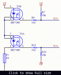
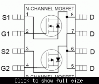
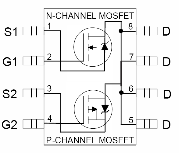
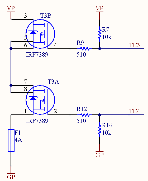
The structure of IRF7389 is as the following:


In one case, I put TC3 in a stable level equal to Vp. When I add pulse(5V 250Hz) on TC4, problem occurs. The current in F1(a fuse) increases greatly at this time and it seems like the two MOSFETs turn on at the same time.

I do not know where is wrong. Please help me! Thanks a lot!
 

Is it correct on the second picture that the drains of the two MOSFETS are connected together?
 

Thanks for your reply!

Yes, it is correct. This picture comes from datasheet of the manufacture. And I have tested that they are really corrected. In fact , I need them to be corrected together. Even the manufacture does not do so, I will wire them together in my circuit.

In fact, the figure above is half of a H-bridge to drive a DC brush-motor. But now, half of the bridge can not work properly, it looks like a short-circuit in it, but I do not know where is wrong.
 

Do you have problems during simulation or with a real circuit? Because on the schematic the P-MOSFET has reversed source and drain, but the pin numbering is ok.
 

short pins 3 and 4 then try you test again . If current wont be increased - decrease resistor impedance values for gate circuits so gate voltage wont be affected by drain to gate capacitance .
 

To Coros:

Thank you very much!

I think the schematic is correct because it is P-Channel MOSFET. Do you think that it should be reversed between pin3 and pin4(5). I don't think so.
 

The source of a P-MOSFET should be more positive than the drain, otherwise the internal diode would conduct current. If VT is the most positive voltage the source should go there, that's why the drains are connected. The gate driving circuit of the half bridge should also be of low impedance, so that the gate capacitances will be charged as quickly as possible and there should be a dead time between switching off one transistor an switching on the other. Open collector driving circuit with a 10k resistor is not a good solution, push-pull would be more adequate.
 

Thank you coros!

In the first schematic drawing, I have tired pin3(Source of P-Channel)to the highest voltage level(Vp, about 12V DC), so I think there is no problem in it.


I wired pin3 and pin4 together just now, and tested the voltage of pin5. It is nearly the same as Vp, that means that the P-Channel MOSFET is ON! Why ? It is so strange. The ON state of P-Channel MOSFET cause the large current when the N-Channel MOSFET is ON. But I do not know why the P-Channel MOSFET is on even when I wired pin3 and pin4 together. I have replaced the chip for one time, the result is the same.
 

Maybe you try to test the P transistor separately for eg. with 12V lamp, just to check if it is not damaged. With source and gate wired together it must be off.
 

RoboColor, did make n channel ON when your P channel was gate-source shorted ? The Vpp could be due to unmatched drain to source leakage current between p and n mosfets .
And what load do you use for tests ?
 

I wired source and gate of p-channel together when I made the test. During the test I put a resistor between drain and ground, I can detect current through the resistor. The current value is about Vp/R.

I will do a test seperately for p-channel tomorrow.

Thanks a lot.
 

Dear all:

I am terrible sorry that the problem is in the device itself. Because I choose a bad dealer, the MOSFET they provide me have more than 50% fault rate. This night, I change the MOSFET(s) for several times, and found that some device could work, and the others not.

I guess that the dealer is selling devices taken down from rubbish PCB board.


So there comes up a question: how to judge if a MOSFET is good before it is soldered on board, with help of multimeter? Thanks a lot.
 

Status
Not open for further replies.

Part and Inventory Search

Welcome to EDABoard.com

Sponsor

Back
Top