yefj
Advanced Member level 4
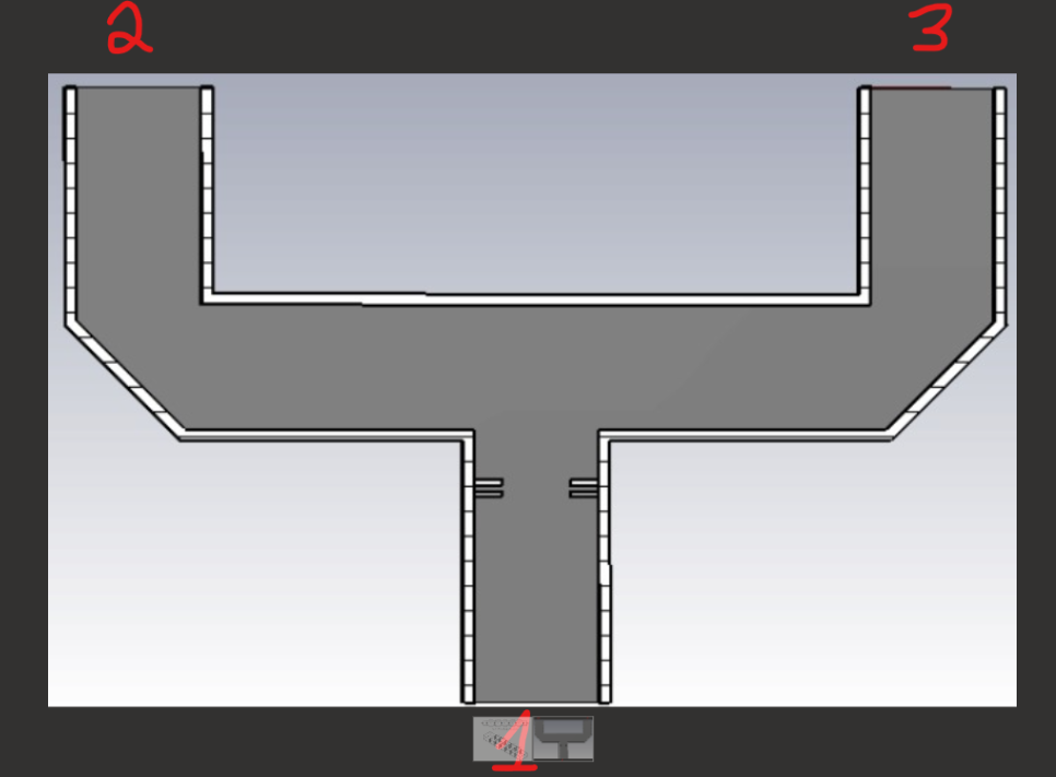
Hello ,i am trying to build a waveguide power divider shown bellow.
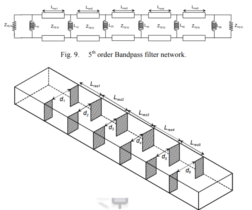
I am trying to use IRIS filtering for wide band matching .
my input is port 1 ,so port 2 and 3 are loads.
so basically the load from port 3 and port 2 are in parallel creating a general total load.
so now i need to create matching network to the load.
given these peaces of metal irises inside the waveguide,how to extract propely the LC model shown bellow.
i have a CST simulation tool.
is there some manual i can read with an example that shows how to convert the E-field and H-fields in the iris model into L-C structure shown bellow?
Thanks.