prcken
Advanced Member level 1
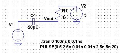
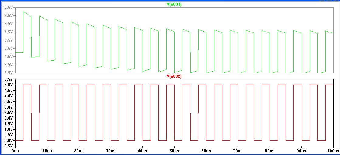
pls look at the images i've uploaded below, can you explain why the amplitude of voltage between the capacitance and resistor finally goes to 2.5V/7.5V
thanks
thanks
Follow along with the video below to see how to install our site as a web app on your home screen.
Note: This feature may not be available in some browsers.
no,V1 is the pulseleehying said:Is V1 same with V2?
jianjing526 said:Initially, c1 is empty, Vc1=0;
V1=0,V2=5,c1 charges;
V1=5,V2=5,c1 discharges;
several periods later. system stable.
Vout is pulse with 2.5-7.5V
jianjing526 said:Well, sorry for the ambiguous answer.
Let's consider the circuit from the concept "system". It's just a RC network with two inspirations marked as V1 and V2. You get the output from the C1. It's actually a low pass system. It has one pole which located at 1/(2pi*RC). If R1=1K, C1=20p, the pole is about 8MHz. Vin has a constant frequency of 200M and about 1.4dec after the pole. Vin attenuates about 28db with reciprocal phase delay. In this situation, the 2.5V-7.5V pulse is not the final stable state. Maybe much more than 20 pulse can help you!
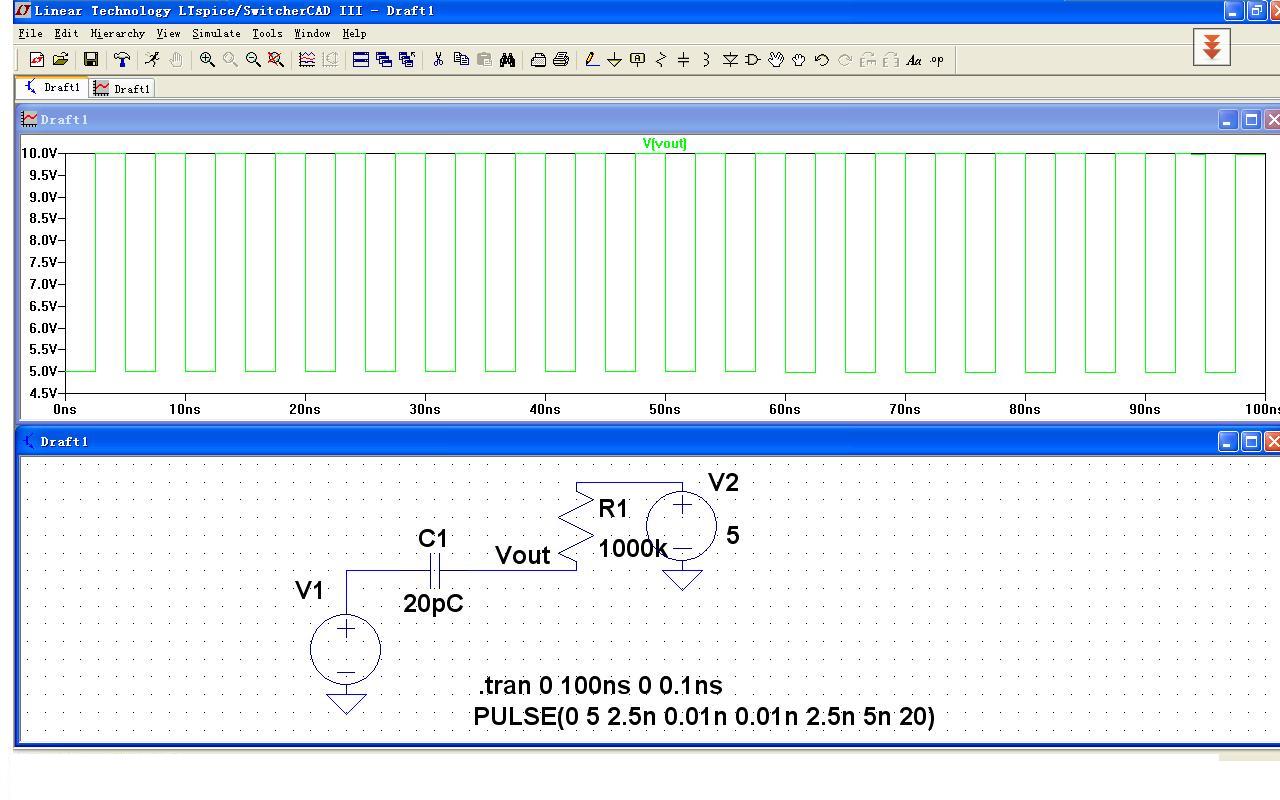
In the second situation, system pole locates at about 8kHz, for a 200M input. AC magnitude is nearly zero. So the C1 voltage is actually dc 5V which appears at the node out to be a 5V-10V pulse!
LvW said:............
3.) The sum of both voltages gives a pulse train between (-2.5+5)=+2.5
and (+2.5+5)=7.5 volts.
4.) This applies for all values of R and C - however, the steady state results
after 5...6 time constants (in your case 20 ns or 20 us, respectively).
Regards.
5.) At t=0: Starting with a positive pulse, both voltages (5+5=10 volts) are added and give a maximum of 10 volts.
6.) There is a smooth transition from t=0 towards the steady state at t>5...6 time constants.
jianjing526 said:Two clearer menthods is described.
1. we consider this from the capacitor C1. C1 charges and discharges periodically with different current rate. Charging current is larger compared to discharging current. So charge in C1 is getting more and more, finally to be a stable value.
2. signal processing: we write the transfer function of the system in s-domain. Then input is added. we got a response at the node out. The final response includes two components, steady one and temporary one.
Anyway, the simulation result you got from the output seems meaningless. The voltage across the capacitor C1 is helpful.
Regards!
what do u mean independent .....and e function, can you kindly give me some statistically deduction? i was stucked at there for a long time, thanksLvW said:。。。。。。。。。。。。。。 always follows an e-function.