Continue to Site

Welcome to EDAboard.com

Welcome to our site! EDAboard.com is an international Electronics Discussion Forum focused on EDA software, circuits, schematics, books, theory, papers, asic, pld, 8051, DSP, Network, RF, Analog Design, PCB, Service Manuals... and a whole lot more! To participate you need to register. Registration is free. Click here to register now.

[SOLVED] help reading 4N26 datasheet (opto-coupler)

Status
Not open for further replies.

bagusdj

Member level 3
Joined
Nov 25, 2012
Messages
67
Helped
0
Reputation
0
Reaction score
0
Trophy points
1,286
Activity points
1,766
Hi guys, I want to ask about getting right value based on datasheet reading

View attachment 4n26.pdf

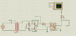
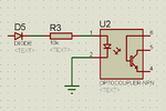
here is the suggested interfacing method.

opto1.png

what i see here:
1. 1 is pin 1, 2 is pin 2, 3 is pin 5, 4 is pin 6.
2. the output is going to MCU at89s52 (the output must have less or equal to 10mA), 2 & 4 goes to ground (but not the same ground; 4 goes to MCU's ground while other goes to input's ground)
3. pin 3 & 6 is not connected.

what i want to ask, what voltage should be applied to input? based on data sheet mentioned max of iF is 80mA,but in other tables mentioned typical and max voltage WHEN iF=10mA. which one i have to assign, so i know what is the value of Rd.

for other side, it said vcc (5Volt); what is the value of current required in 3 (pin 5)?
 

You conclusion 1/2/3 should be o.k. The purpose on a opto coupler is to isolate two systems(GND and Vcc). The MCU output is driving the diode side and the photo transistor the isolated system side. For the other direction it is just opposite. The absolute maximum ratings in the data sheet is not the operating condition. These are the electrical characteristics(e.g. IF=10mA with max. 1.5V VF. RD must be selected to meet the output drive capability of the I/O port. The normal MCU I/O ports can't drive 10mA on the high side. The possible 4N26 transistor current depends on IL and CTR. The datasheet specifies minimal 2mA with IF=10mA. So this is not very much and you might need additional driver. Here you find application examples for interfacing the microcontroller to the outside world: https://www.ichaus.biz/wp1_mcu_interface .

Enjoy your design work!

i dont get it (the bold one)

should I give 10mA or 2 mA then? :s

thanks anyway :D

any other points of view?
 

That means that if you drive the diode with 10mA current you get a minimum of 2mA in the output of the opto (up to 5mA typical)
 

That means that if you drive the diode with 10mA current you get a minimum of 2mA in the output of the opto (up to 5mA typical)

hmmm... is it right if i say this way:

1. the max voltage that allowed to pass through led is 1.5V, and I should put RD not more than 150 Ohm; thus i get the iF=10mA.
2. by applying iF=10mA, i will get 2mA in collector side (which will goes through mcu and its a suffice value). In the output side, there is vcc (since its vcc,then its 5V) and I should put RL 500 Ohm to make it 10mA maximum (max current that allowed to pass through MCU).

how then to get 1.2-1.5 Volt to feed the led? i know voltage would drop after passing rectifier (fyi, i will feed the led with ac source to detect its zero crossing and give the output side to mcu). since 1.5 is the maximum allowed voltage.

is it like that?
 

There is no max voltage specification for the diode, just a max current which is 80mA.
There is only a max reverse voltage spec which is 6v

If you are going to use AC then you should use an diode in series with the internal diode and a resistor.

The resistor will be R= (Vin - Vf_diode - Vf opto) / I

fyi this is the schematic that i use to test zdc


by putting a diode series, is it like this? and the R that you mean is the R in diode side right?
what is the correlation between ac source and diode?
 

Attachments

  • zcd.png
    zcd.png
    22.8 KB · Views: 102
  • opto.png
    opto.png
    7.6 KB · Views: 113

the external diode is used to prevent the reverse polarity voltage to reach the opto diode to protect it (the inverted voltage limit is 6v)
 

Status
Not open for further replies.

Similar threads

Part and Inventory Search

Welcome to EDABoard.com

Sponsor

Back
Top