Welcome to our site! EDAboard.com is an international Electronics Discussion Forum focused on EDA software, circuits, schematics, books, theory, papers, asic, pld, 8051, DSP, Network, RF, Analog Design, PCB, Service Manuals... and a whole lot more! To participate you need to register. Registration is free. Click here to register now.
You are going to have to be *much* more specific than that. Use google to do some research, buy a book - I found that 'The Art of electronics', Horowitz and Hill is a good starter.
Thanks for your help, these books gives you info about electronic devices but i need to know how to calculate the values of different passive elements according to the required power
you must have powerful knowledge about circuit theorem. there are some network related theorem that you have to learn. for example nodal analysis, mesh analysis, nortan theorem etc.
hi all
you also need to know about circuit transient , mutual inductance , two port networks , and the most important control theory to learn how to control your cct.
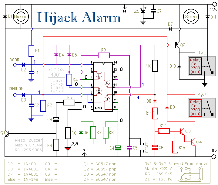
Does this work ??? i had a look at the data sheet for CMOS 4001 and that says pin 14 must b having input voltage of around 3 to 15... if am wrong please dnt mind... Let me know that answer
Here you have situation when every think is OK.
The Door is close
So when door is close Q3 and Q4 are ON and relay Ry2 is ON to.
And now when someone open the door the situation will look like this.
So we have High state on output of a first gate.
The red LED is ON.
HIGH state begins the process of charging the capacitor C3, so Q1 stay "ON" (buzzer is also ON) until C3 is fully charged. After that Q1/buzzer is off.
At the same time C4 is charging through R6, R7.
And when C4 charge to 0.5Vdd the output of a 3 gate gos to LOW state. And this will causes Q2 to ON and Ry1 also ON. So buzzer and Siren will be ON to.
The LOW state on output of a third gate will off Q3, Q4 (there will be some delay thanks to C6).
And LOW state on output off a fourth gate will locks the circuit in this state.
Until the door is close and reset button is press.
This site uses cookies to help personalise content, tailor your experience and to keep you logged in if you register.
By continuing to use this site, you are consenting to our use of cookies.

")