Continue to Site

Welcome to EDAboard.com

Welcome to our site! EDAboard.com is an international Electronics Discussion Forum focused on EDA software, circuits, schematics, books, theory, papers, asic, pld, 8051, DSP, Network, RF, Analog Design, PCB, Service Manuals... and a whole lot more! To participate you need to register. Registration is free. Click here to register now.

help me to analyze the circuit

Status
Not open for further replies.

liucheng311

Junior Member level 3
Joined
Jul 15, 2009
Messages
28
Helped
0
Reputation
0
Reaction score
0
Trophy points
1,281
Location
China
Activity points
1,466
dear everyone
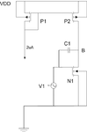
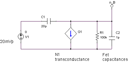
i want to know about zeros of circuit,so i build a circuit shown below:the capacitance of C1 is about 20pF;V1 is a sin signal,its offset voltage is 1V,and its amplitude voltage is 10mV.when the frequency of V1 is higher than about 1MHZ,the voltage at node B is a sin wave,whose peak-peak value is 20mV,and the higher peak voltage is 1.92V,which is the operating point.
i know at higher frequency,the capacitor will short the gate and node B,but why is the higher peak voltage at node B at its operating point?
 

Attachments

  • 电容仿真.png
    电容仿真.png
    12.7 KB · Views: 136

Hello,

The capacitor doesn't short the gate as you drive from a voltage source, so gate voltage is constant. for frequencies where Y of capacitor is large w.r.t. Gm, Vb will be determined by the capacitive division between C1 and the other mosfet capacitances. You should put a resistor in series with the voltage source in my opinion.

For High frequency, Vb will be almost in phase with Vgate.
 
wimRFP,thanks for your replying.
quote:Vb will be determined by the capacitive division between C1 and the other mosfet capacitances.
but the higher peak voltage at node B is always at its operating point as long as the frequency of V1 is high enough,when i change the capacitance of C1.how do you explain this?
 

Hello,

When all mosfet capacitances are very small with respect to C1 and frequency is high enough, v1 = vb, so 10mV input give 20mV pp at b. So your observation regarding the AC voltages is OK.

To avoid confusion, can you clarify "and the higher peak voltage is 1.92V, which is the operating point" (with a graph?).
 
thanks,WimRFP,
sorry for replying so late,my network is not always available.
for the "operating point",i mean the resulted voltage by applying a dc power on the gate.
you said"Vb will be determined by the division between C1 and the other mosfet capacitance ",could you explain it concretely?thx!
 

I am sorry, but I still don't understand your sentence: "and the higher peak voltage is 1.92V, which is the operating point".

Regarding the AC voltage in B due to V1
Imagine that from B to ground (or VDD) there is 1 pF capacitance (see it as fet capacitances, modelled as C1 in the imgage).
90_1314021724.png


So we have a series circuit of C1 (20pF) and 1pF to ground. However from B to ground there is also the output impedance of the current mirror (P2) and N1, all modelled as R1). There is also a controlled current source (N1's transconductance, modelled as G1). `

For low frequency, the behavior is dominated by N1's transconductance and R1 (as you can ignore the capacitances).

At very high frequency, X(C1) << R1, and X(C1) << 1/G(n1), so R1 and 1/G can be ignored. In other words, all current flowing into C1 goes through C2 and a capacitive voltage divider has been created. X(..) = reactance of.

Vb = V1(10p/(10p+1p) ) = 0.91*V1.

So if V1 = 10 mVp, Vb = 9.1mVp (that is 18.2mVpp). This AC voltage is centered around the DC bias voltage in B (ignoring non-linearity of the fet characteristics). If the fet capacitances are less (so C1 has lower value), voltage in B will increase to maximum 20mVpp.
 
What is your Vdd voltage? I wonder how you manage to keep the operating point at the output without having any sort of DC feedback? After all at the output you have two current sources connected at a high-impedance node and any mismatch in the currents will rail the stage.
 
Last edited:
hello,WimRFP
for "the operating point", i mean the DC bias voltage. i am not good at english,sorry to make you confused.as you said "This AC voltage is centered around the DC bias voltage in B",i found the AC voltage is below the DC bias voltage in B,maybe that is because i didnot manage to keep the operating point as sutapanaki said.
and thank you for your modeling,that is very clear!

hello,sutapanaki
thank you for your reminding,i am not sure i manage to keep the operating point since the circuit does not have any sort of DC feedback,i will check it
 

Status
Not open for further replies.

Similar threads

Part and Inventory Search

Welcome to EDABoard.com

Sponsor

Back
Top