swapan
Full Member level 4
Hi friends,
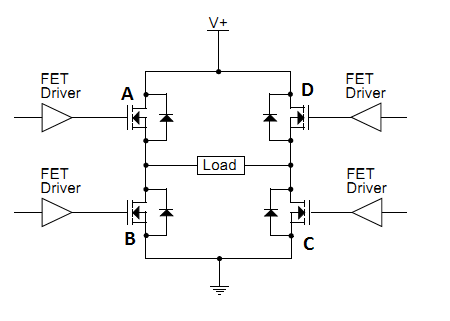
After having basic inputs from this forum regarding sine wave inverter employing H Bridge, I have come to the conception that high side MOSFETs are driven by pulse of 50Hz signal and low side MOSFETs are driven by PWM pulse of carrier frequency. Please rectify me if the conception is wrong.
To prevent shoot through current during transition period, dead-band delay is incorporated. Please let me know which signal is to be delayed, high frequency pulse or low frequency pulse?
During charging process, the induced voltage depends on duty cycle of applied signal. Please state the typical value of frequency of the signal applied to the boost converter.
Regards
swapan